Review
. 2023 Nov 10;5(2):804-817.
doi: 10.1016/j.fmre.2023.10.008. eCollection 2025 Mar.

Gallium oxide (Ga2O3) heterogeneous and heterojunction power devices

Affiliations
Review

Gallium oxide (Ga2O3) heterogeneous and heterojunction power devices

Bochang Li et al. Fundam Res. .

Abstract

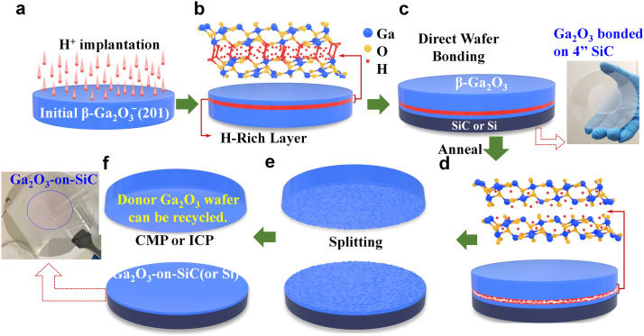
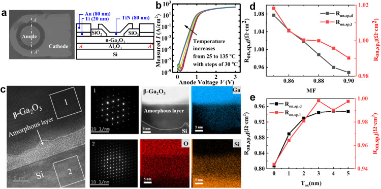
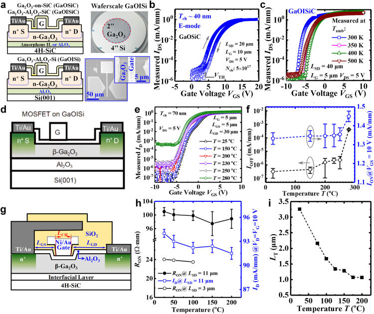
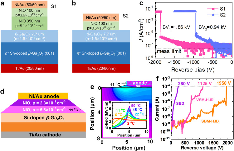
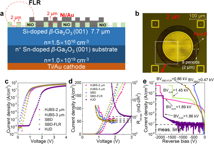
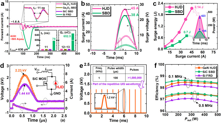
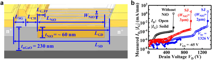
Due to its high critical breakdown electrical field and the availability of large-scale single crystal substrates, Gallium oxide (Ga2O3) holds great promise for power electronic and radio frequency (RF) applications. While significant advancements have been made in Ga2O3 material and device research, there are still challenges related to its ultra-low thermal conductivity and the lack of effective p-type doping methods. These limitations hinder the fabrication of complex device structures and the enhancement of device performance. This review aims to provide an introduction to the research development of Ga2O3 heterogeneous and heterojunction power devices based on heterogeneous integration technology. By utilizing ion-cutting and wafer bonding techniques, heterogeneous substrates with high thermal conductivity have been realized, offering a viable solution to overcome the thermal limitations of Ga2O3. Compared to Ga2O3 bulk devices, Ga2O3 devices fabricated on heterogeneous substrates integrated with SiC or Si exhibit superior thermal properties. Power diodes and superjunction transistors based on p-NiO/n-Ga2O3 heterojunctions on heterogeneous substrates have demonstrated outstanding electrical characteristics, presenting a feasible method for the development of bipolar devices. The technologies of heterogeneous integration and heterojunction address critical issues related to Ga2O3, thereby advancing the commercial applications of Ga2O3 devices in power and RF fields. By integrating Ga2O3 with other materials and leveraging heterojunction interfaces, researchers and engineers have made significant progress in improving device performance and overcoming limitations. These advancements pave the way for the wider adoption of Ga2O3-based devices in various power and RF applications.

Keywords: Ga2O3; Heterogeneous integration; Heterojunction; NiO; Superjunction.


Conflict of interest statement

The authors declare that they have no conflicts of interest in this work.

Figures

Fig 1
Fig. 1
The process flow for transferring β-Ga2O3 thin film onto SiC (or Si) by ion cutting. (a)-(b) Implanting H+ into bulk β-Ga2O3 to form the H-rich layer. (c) Wafer bonding of β-Ga2O3 with SiC (or Si), and bonding interfacial layer (IL) can be an amorphous layer or an Al2O3 film. (d) Forming plate-like defects by annealing. (e) Splitting. (f) Surface smoothing by ICP etching or CMP. Fabricated GaOSiC is shown . © [2021] IEEE. Reprinted, with permission, from .
Fig 2
Fig. 2
Surface blistering of β-Ga2O3 bulk wafers through H ion implantation. (a) In situ OM images of the surface variation of H-implanted β-Ga2O3 bulk annealed at 480 °C, (b) total free energy versus radius of the hydrogen blister with different internal pressures, (c) Arrhenius plot of the blistering time as a function of the annealing temperature, and (d) time for surface blistering versus heating temperature with different values of implantation fluence. Adapted with permission from . Copyright 2021, American Chemical Society.
Fig 3
Fig. 3
The XTEM image of β-Ga2O3/SiC heterogeneous integration materials based on different bonding methods. (a) surface activated bonding , (b) Hydrophilic bonding . Reprinted from , with the permission of AIP Publishing.
Fig 4
Fig. 4
A 2-inch single-crystalline Ga2O3 thin film transferred onto Si and SiC substrates. (a) The photograph of a 2-inch β-Ga2O3 thin film transferred onto SiC handle wafer and the exfoliated β-Ga2O3 bulk wafer, (b) the thickness mapping of the β-Ga2O3 thin film , Panels (a) and (b) adapted with permission from . Copyright 2021, American Chemical Society. (c) the normalized (2¯01) XRCs of the β-Ga2O3 thin film before and after a post-annealing process, (d) AFM image of the β-Ga2O3 thin film after CMP process .
Fig 5
Fig. 5
Ga2O3 heterogeneous SBDs. (a) The optical image of fabricated β-Ga2O3/TiN SBD and device structure . (b) Temperature-dependent I-V characteristics of the β-Ga2O3/TiN SBD with a stable ION/IOFF ratio. Panels (a) and (b) reproduced with permission from . Copyright 2020, IOP Publishing Ltd. (c) Cross-sectional TEM microscope image of Ga2O3/Si interface and the EDS spectrum of Ga, O and Si at the interface . (d) Comparison of Ron,sp,d and Ron,sp,l of Ga2O3/Si SBDs with different Mole Fraction (MF). (e) comparison of Ron,sp,d and Ron,sp,l of Ga2O3/Si SBDs with different amorphous layer thickness (Tox).
Fig 6
Fig. 6
Ga2O3 heterogeneous MOSFETs. (a) Schematics of the heterogeneous Ga2O3 MOSFETs fabricated on the heterogeneous wafers . (b) The transfer characteristics of an E-mode GaOSiC MOSFET with a Tch of ∼40 nm. (c) Transfer characteristics of a GaOISiC MOSFET measured at different ambient temperatures (Tamb). © [2021] IEEE. Panels (a), (b) and (c) Reprinted, with permission, from . (d) Schematic of the heterogeneous GaOISi MOSFET . (e) Transfer characteristics of a D-mode GaOISi MOSFET measured at different temperatures. (f) Dependence of ION and IOFF on the temperature. Panels (d), (e) and (f) Reproduced with permission from Springer Nature, copyright 2020. (g) Schematic of the recessed-gate GaOSiC MOSFET . (h) Temperature dependence of RON and drive current of the recessed-gate GaOSiC MOSFET. (i) The evolution of transfer length at the electrode contacts with the temperature. © [2022] IEEE. Panels (g), (h) and (i) Reprinted, with permission, from .
Fig 7
Fig. 7
Channel mobility properties of Ga2O3 heterogeneous MOSFETs. (a) The transfer characteristics of the GaOISi MOSFETs with different channel thickness . © [2021] IEEE. Reprinted, with permission, from . (b) Calculated µeff vs Qch for GaOISi MOSFETs with the different channel thickness. Benchmarking µeff of (c) GaOISi and (d) GaOSiC MOSFETs with the reported µH and µeff of β-Ga2O3 materials and devices ,. (e) Calculated µFE for the accumulated GaOSiC MOSFET as Tamb increases from 0 °C to 150 °C . © [2021] IEEE. Reprinted, with permission, from .
Fig 8
Fig. 8
NiO/Ga2O3 heterojunction power diode. Schematic cross-section of (a) double-layered and (b) single-layered NiO/Ga2O3 HJD. (c) Breakdown characteristics of HJD in (a) and (b) . Reprinted from , with the permission of AIP Publishing. (d) NiO/Ga2O3 heterojunction with beveled mesa . (e) Simulated electric field distributions of NiO/Ga2O3 HJD with varying bevel angle. (f) Reverse I-V characteristics . © [2022] IEEE. Reprinted, with permission, from .
Fig 9
Fig. 9
NiO/Ga2O3 HJBS diodes. (a) Schematic cross-section of NiO/Ga2O3 HJBS with FLRs. (b) Top-view microscopy image. (c) Semi-logarithmic J-V characteristics. (d) Linear J–V characteristics and extracted Ron,sp as a function of forward bias. (e) Reverse J-V characteristics. Reprinted from , with the permission of AIP Publishing.
Fig 10
Fig. 10
Dynamic electrical characteristics of NiO/Ga2O3 heterojunction power diodes. (a) Reverse recovery characteristics and (b) Surge current characteristics of the 9-mm2 HJD and SBD . © [2021] IEEE. Reprinted, with permission, from . (c) Corresponding surge power and energy. (d) The UIS current and voltage waveforms of the HJD. (e) Repetitive UIS characteristics . (f) System efficiency vs. output power of a 500-W PFC circuit at a switching frequency of 0.1 MHz and 0.5 MHz . © [2022] IEEE. Reprinted, with permission, from .
Fig 11
Fig. 11
Ga2O3 based SJ-MOSFET,. Schematic cross-section of (a) SJ-MOSFET. (b) Reverse J-V characteristics. © [2021] IEEE. Reprinted, with permission, from ,.

Similar articles

Cited by

References

    1. Pearton S., Ren F., Mastro M. Elsevier; 2018. Gallium Oxide: Technology, Devices and Applications.
    1. Green A.J., Speck J., Xing G., et al. β-Gallium oxide power electronics. APL Mater. 2022;10
    1. Chang P.-C., Fan Z., Tseng W.-Y., et al. β-Ga2O3 nanowires: Synthesis, characterization, and p-channel field-effect transistor. Appl. Phys. Lett. 2005;87
    1. Matsuzaki K., Yanagi H., Kamiya T., et al. Field-induced current modulation in epitaxial film of deep-ultraviolet transparent oxide semiconductor Ga2O3. Appl. Phys. Lett. 2006;88
    1. Matsuzaki K., Hiramatsu H., Nomura K., et al. Growth, structure and carrier transport properties of Ga2O3 epitaxial film examined for transparent field-effect transistor. Thin. Solid. Films. 2006;496:37–41.

LinkOut - more resources