Review
. 2025 May;12(19):e2413131.
doi: 10.1002/advs.202413131. Epub 2025 Apr 17.

The Rise of Chalcohalide Solar Cells: Comprehensive Insights From Materials to Devices

Affiliations
Review

The Rise of Chalcohalide Solar Cells: Comprehensive Insights From Materials to Devices

Hongrui Zhang et al. Adv Sci (Weinh). 2025 May.

Abstract

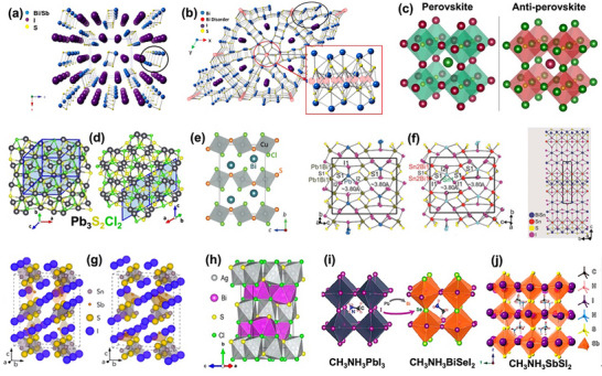
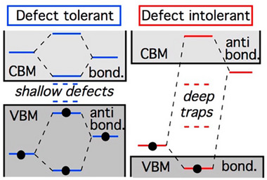
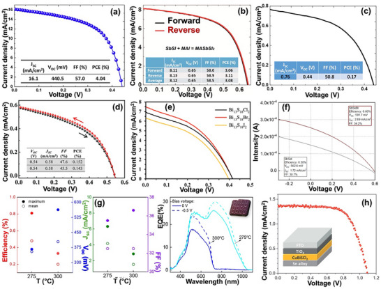
While lead-halide perovskites achieve high efficiencies, their toxicity and instability drive the search for safer materials. Chalcohalides, combining chalcogen and halogen anions in versatile structures, emerge as earth-abundant, nontoxic alternatives for efficient photovoltaic (PV) devices. A wide variety of chalcohalide materials, including pnictogen metals-, post-transition metals-, mixed-metals- and organic-inorganic metals-based chalcohalides, offer diverse structural, compositional, and optoelectronic characteristics. Some of these materials have already been experimentally synthesized and integrated into PV devices, achieving efficiencies of 4-6%, while others remain theoretically predicated. Despite these advancements, significant challenges must be addressed to fully realize the potential of chalcohalides as next-generation PV absorbers. This review provides a comprehensive insight of the fundamental properties of chalcohalide materials, emphasizing their unique structures, highly interesting optoelectronic and dielectric properties, to fuel further research and guide the development of high-efficiency chalcohalide solar cells. Various synthesis techniques are discussed, highlighting important and potentially overlooked strategies for fabricating complex quaternary and pentanary chalcohalide materials. Additionally, the working principles of different device structures and recent advances in fabricating efficient chalcohalide solar cells are covered. We hope that this review inspires further exciting research, innovative approaches, and breakthroughs in the field of chalcohalide materials.

Keywords: metal chalcohalides; perovskite‐inspired semiconductors; solar absorber; thin film photovoltaics.


Conflict of interest statement

The authors declare no conflict of interest.

Figures

Figure 1
Figure 1
The evolution of device efficiencies of various chalcohalide solar cells.
Figure 2
Figure 2
a) Structure of BiSI looking down the b‐axis at the ac‐plane. The black circle highlights the Bi–S 1‐D chain.[ 35a ] b) Averaged cell representation (ACR) of the hexagonal P63 structure of Bi13S18I2 viewed down the c‐axis. Inset: normal to the c‐axis to highlight bismuth (disordered/averaged dimer) sites, in hatched red.[ 36a ] c) Schematic representation of the perovskite and antiperovskite crystal structure. Both are isostructural but with anions in place of cations and vice versa.[ 24c ] d) Two views of the Cc monoclinic Pb3S2Cl2 structure ([100] left, [111] right).[ 23i ] e) Atomic structure of CuBiSCl2.[ 23h ] f) Crystal structures of Pb2BiS2I3 (left) and Sn2BiSI5 (middle, right).[ 43 ] g) Calculated crystal structures for Cmcm and Cmc21 polymorphs of Sn2SbS2I3.[ 16c ] h) Crystal structure of AgBiSCl2, highlighting the coordination of both Ag and Bi atoms and the formation of alternate layers.[ 47a ] i) Atomic structures of CH3NH3PbI3 (left) and CH3NH3BiSeI2 (right).[ 58 ] j) Crystal structure of CH3NH3SbSI2.[ 59 ] Reproduced with permission.[ 35a ] Copyright 2017, American Chemical Society. Reproduced with permission.[ 36a ] Copyright 2017, American Chemical Society. Reproduced with permission.[ 24c ] Copyright 2022, Wiley. Reproduced with permission.[ 23i ] Copyright 2020, Nature. Reproduced with permission.[ 23h ] Copyright 2022, Wiley. Reproduced with permission.[ 43 ] Copyright 2016, American Chemical Society. Reproduced with permission.[ 16c ] Copyright 2021, Royal Society of Chemistry. Reproduced with permission.[ 47a ] Copyright 2023, American Chemical Society. Reproduced with permission.[ 58 ] Copyright 2016, Royal Society of Chemistry. Reproduced with permission.[ 59 ] Copyright 2018, American Chemical Society.
Figure 3
Figure 3
a) The dashed line represents a linear extrapolation of the trend toward BiSeI.[ 23a ] b) Indirect bandgap of BiOBr1−xIx and BiSBr1−xIx.[ 15b ] c) UV–vis–NIR absorption spectra of Bi13S18X2 powder samples.[ 38 ] Reproduced with permission.[ 23a ] d) Absorption spectra of Ag3SBr and Ag3SI films by PDS.[ 23j ] e) Bandgap as a function of x (Br amount).[ 23j ] f) UV/vis absorption spectrum of polycrystalline powder of Pb2BiS2I3, Sn2BiS2I3, Pb2SbS2I3, “Pb2Sb1− x Bi x S2I3” (x ≈0.4), and Sn2BiSI5. The bump at ≈1.5 eV in the red spectrum (Sn2BiS2I3) is due to the detector switch which we see frequently in different samples. g–i) projected electronic density of states of g) Pb2BiS2I3 h) Sn2BiS2I3 i) Sn2BiSI5.[ 43 ] Copyright 2020, American Chemical Society. Reproduced with permission.[ 15b ] Copyright 2016, Nature. Reproduced with permission.[ 38 ] Copyright 2021, American Physical Society. d,e) Reproduced with permission.[ 23j ] Copyright 2024, Royal Society of Chemistry. f–i) Reproduced with permission.[ 43 ] Copyright 2016, American Chemical Society.
Figure 4
Figure 4
a) Indirect bandgap Tauc plots of solid‐state UV–vis Kubelka–Munk diffuse reflectance spectra for Sn2SbS2−xSexI3.[ 44 ] b) UV–vis spectra and Tauc plots of Ag3BiI6‐2xSx.[ 31b ] c) Density of states of CH3NH3PbI3 and CH3NH3BiSI2 (left) and calculated bandgaps of CH3NH3PbI3 and CH3NH3BiSeI2 (middle, right).[ 58 ] d) Tauc plots of CH3NH3BiSI2.[ 50 ] Reproduced with permission.[ 31b ] Copyright 2018, Wiley. Reproduced with permission.[ 44 ] Copyright 2023, Royal Society of Chemistry. Reproduced with permission.[ 58 ] Copyright 2016, Royal Society of Chemistry. Reproduced with permission.[ 50 ] Copyright 2019, The Chemical Society of Japan.
Figure 5
Figure 5
a) formation energies per atom (upper panel), band gaps (middle panel), and effective masses of electron and hole (lower panel) for the 31 Bi and Sb‐based compounds. b) band gaps, hole and electron effective masses as a function of average electronegativity discrepancy between anions and cations for the 31 Bi and Sb‐based compounds; bottom left band gaps, bottom right effective masses of electron and hole as a function of bond valence sum of the cations. c) calculated dielectric constants (ε) of the considered bismuth/antimony oxyhalides and chalcohalides.[ 14a ] a–c) Reproduced with permission.[ 14a ] Copyright 2018, Nature.
Figure 6
Figure 6
Defect tolerance versus defect intolerance.[ 75c ] Reproduced with permission.[ 75c ] Copyright 2014, America Society Chemistry.
Figure 7
Figure 7
Mesoscopic structured solar cell versus n–i–p planar structured solar cell.
Figure 8
Figure 8
Schematic illustration of some solution processes for chalcohalide solar cell fabrication. a) One‐step and two‐step spin‐coating method, b) Chemical deposition method, and c) Spray‐pyrolysis method.
Figure 9
Figure 9
a) IPCE spectra of a film deposited at 275 °C.[ 23b ] b) Short‐circuit IPCE values measured for films with various Se/(S + Se) levels measured in a two‐electrode cell containing I/I2 in acetonitrile.[ 23a ] c) Photoelectrochemical IV curves for films with various Se/(S + Se) levels measured in a two‐electrode cell containing I/I2 in acetonitrile under AM1.5G illumination.[ 23a ] d) IPCE spectra of the BiSI electrode in an acetonitrile solution containing 0.1 M NaI at various applied potentials and absorption spectrum of BiSI.[ 15b ] e) J–V characteristics of 16 devices under AM 1.5G simulated illumination and key performance metrics of the best device.[ 87 ] f) Time‐resolved photoluminescence of BiSI films employing 633 nm excitation, revealing two time‐constants of 0.09 and 1.03 ns.[ 87 ] g) I–V curves of 8 Bi13S18I2‐based solar cells.[ 23c ] h) current density–voltage (J–V) curves of BiSI.[ 85 ] i) J–V curves of the five solar cell devices.[ 88 ] Reproduced with permission.[ 23b ] Copyright 2012, American Chemical Society. b,c) Reproduced with permission.[ 23a ] Copyright 2012, American Chemical Society. Reproduced with permission.[ 15b ] Copyright 2016, Nature. e,f) Reproduced with permission.[ 87 ] Copyright 2019, American Chemical Society. Reproduced with permission.[ 23c ] Copyright 2020, Royal Society of Chemistry. Reproduced with permission.[ 85 ] Copyright 2020, American Chemical Society. Reproduced with permission.[ 88 ] Copyright 2021, Wiley.
Figure 10
Figure 10
a) Incident photon to current conversion efficiency at a 0.25 V bias under monochromatic illumination.[ 69 ] b) J–V curves under standard illumination conditions (100 mW cm−2) of air mass 1.5 global (AM 1.5G).[ 23d ] c) external quantum efficiency (EQE) spectrum of the SbSI devices with various HTMs.[ 23d ] d) photovoltaics efficiency of SbSI.[ 83a ] e,f) IPCE spectrum and UV–vis absorption spectrum of the ASBSI devices fabricated via CBD of Sb2S3 for 2.5, 3.0, and 3.5 h, respectively.[ 30 ] g) The cross‐sectional FESEM image of the device fabricated via CBD of Sb2S3 for 3.5 h.[ 30 ] h) Schematic diagram to explain the effect of the ASBSI amount on the infiltration of HTM.[ 30 ] Reproduced with permission.[ 69 ] Copyright 2022, Wiley. b,c) Reproduced with permission.[ 23d ] Copyright 2018, Wiley. Reproduced with permission.[ 83a ] Copyright 2018, AIP publishing. e–h) Reproduced with permission.[ 30 ] Copyright 2019, Wiley.
Figure 11
Figure 11
a) the schematic comparison of solution process and vapor process in formation mechanism, operating principle and cross‐sectional SEM image.[ 89 ] b) two ways to enhance charge transfer.[ 89 ] c) The architecture of photovoltaic device containing SbSI‐PAN nanocomposite (left) and its energy level diagram (right).[ 82 ] d) J–V curves under standard illumination conditions (100 mW cm−2) of AM 1.5 G and e) IPCE spectra of SbSeI solar cells fabricated through 8, 10, and 12 spin‐coating cycles and thermal decomposition.[ 90 ] a,b) Reproduced with permission.[ 89 ] Copyright 2022, Wiley. Reproduced with permission.[ 82 ] Copyright 2020, Elsevier. d,e) Reproduced with permission.[ 90 ] Copyright 2021, Wiley.
Figure 12
Figure 12
a) Current–voltage curve under AM1.5G illumination for a solar cell Inset: Photo of a representative sample.[ 23i ] b) Optical absorption spectra of the three samples.[ 23i ] c) Absorption spectra of Ag3SBr and Ag3SI films by PDS d) Bandgap as a function of x (Br amount).[ 23j ] e) J–V curves under standard test condition (STC).[ 31a ] f) Schematic diagrams of energy levels for the device to describe the role of trap states.[ 31a ] g) (a) open‐circuit voltage, (b) short‐circuits current density, (c) fill factor, and (d) power conversion efficiency of the Au|PTAA|Ag3BiI6−2xSx | m‐TiO2|c‐TiO2|FTO solar cells.[ 31b ] a,b) Reproduced with permission.[ 23i ] Copyright 2020, American Chemical Society. c,d) Reproduced with permission.[ 23j ] Copyright 2024, Royal Society of Chemistry. e,f) Reproduced with permission.[ 31a ] Copyright 2018, American Chemical Society. Reproduced with permission.[ 31b ] Copy 2019, Wiley.
Figure 13
Figure 13
a) Current density–voltage curve of the champion Sn2SbS2I3 solar cell.[ 31b ] b) J–V curves in forward‐ and reverse‐scan modes of the champion MASbSI2.[ 49 ] c) The J–V curves without MASbSI2.[ 49 ] d) Forward and backward scanning of the reaction 30 min of MA3Bi2I9−2xSx.[ 48a ] e) J–V curve of Bi13S18X2 with optimal Bi13S18X2 thickness.[ 38 ] f) intensity–voltage curves of SbSeBr and SbSeI prototype solar cells.[ 40 ] g) Optoelectronic parameters of MoSbSeI/CdS/i‐ZnO/ITO solar cells under different annealing conditions: PCE and Voc (left), Jsc and FF (middle), EQE (right) (with applied 0 V and −0.5 V).[ 40 ] h) J–V curve measured on a CuBiSCl2 based solar cell. The inset shows the schematic structure of the device.[ 23h ] Reproduced with permission.[ 31b ] Copyright 2019, Cell. b,c) Reproduced with permission.[ 49 ] Copyright 2018, American Chemical Society. Reproduced with permission.[ 48a ] Copyright 2019, Wiley. Reproduced with permission.[ 38 ] Copyright 2021, American Physical Society. f,g) Reproduced with permission.[ 40 ] Copyright 2023, Royal Society of Chemistry. Reproduced with permission.[ 23h ] Copyright 2019, Wiley.

Similar articles

References

    1. a) Jeon N. J., Noh J. H., Kim Y. C., Yang W. S., Ryu S., Seok S. I., Nat. Mater. 2014, 13, 897; - PubMed
    2. b) Hao F., Stoumpos C. C., Cao D. H., Chang R. P., Kanatzidis M. G., Nat. Photonics 2014, 8, 489;
    3. c) Saparov B., Mitzi D. B., Chem. Rev. 2016, 116, 4558; - PubMed
    4. d) Correa‐Baena J.‐P., Saliba M., Buonassisi T., Grätzel M., Abate A., Tress W., Hagfeldt A., Science 2017, 358, 739; - PubMed
    5. e) Han T. H., Tan S., Xue J., Meng L., Lee J. W., Yang Y., Adv. Mater. 2019, 31, 1803515; - PubMed
    6. f) Xiao Z., Song Z., Yan Y., Adv. Mater. 2019, 31, 1803792; - PubMed
    7. g) Tong Y., Najar A., Wang L., Liu L., Du M., Yang J., Li J., Wang K., Liu S., Adv. Sci. 2022, 9, 2105085. - PMC - PubMed
    1. a) Woo J., Christian A. H., Burgess S. A., Jiang Y., Mansoor U. F., Levin M. D., Science 2022, 376, 527; - PMC - PubMed
    2. b) Liu C., Yang Y., Chen H., Xu J., Liu A., Bati A. S., Zhu H., Grater L., Hadke S. S., Huang C., Science 2023, 382, 810; - PubMed
    3. c) Chen H., Liu C., Xu J., Maxwell A., Zhou W., Yang Y., Zhou Q., Bati A. S., Wan H., Wang Z., Science 2024, 384, 189. - PubMed
    1. a) National Renewable Energy La boratory (NREL), Interactive Best Research‐Cell Efficiency Chart, https://www.nrel.gov/pv/interactive‐cell‐efficiency.html (accessed: March 2025);
    2. b) Shi Y., Berry J. J., Zhang F., ACS Energy Lett. 2024, 9, 1305;
    3. c) Liu S., Lu Y., Yu C., Li J., Luo R., Guo R., Liang H., Jia X., Guo X., Wang Y.‐D., Nature 2024, 628, 306; - PubMed
    4. d) Lim J., Park N.‐G., Il Seok S., Saliba M., Energy Environ. Sci. 2024, 17, 4390. - PMC - PubMed
    1. a) Seok S. I., Grätzel M., Park N. G., Small 2018, 14, 1704177; - PubMed
    2. b) Liu J., Zheng D., Wang K., Li Z., Liu S., Peng L., Yang D., Joule 2024, 8, 944;
    3. c) Park N.‐G., Zhu K., Nat. Rev. Mater. 2020, 5, 333;
    4. d) Li Z., Klein T. R., Kim D. H., Yang M., Berry J. J., Van Hest M. F., Zhu K., Nat. Rev. Mater. 2018, 3, 18017;
    5. e) Zhu P., Chen C., Dai J., Zhang Y., Mao R., Chen S., Huang J., Zhu J., Adv. Mater. 2024, 36, 2307357. - PubMed
    1. a) Kim H.‐S., Seo J.‐Y., Park N.‐G., ChemSusChem 2016, 9, 2528; - PubMed
    2. b) Wang D., Wright M., Elumalai N. K., Uddin A., Sol. Energy Mater. Sol. Cells 2016, 147, 255;
    3. c) Tiep N. H., Ku Z., Fan H. J., Adv. Energy Mater. 2016, 6, 1501420;
    4. d) Rong Y., Liu L., Mei A., Li X., Han H., Adv. Energy Mater. 2015, 5, 1501066;
    5. e) Ono L. K., Qi Y., Liu S., Joule 2018, 2, 1961;
    6. f) Zhuang J., Wang J., Yan F., Nano‐Micro Lett. 2023, 15, 84; - PMC - PubMed
    7. g) Wang Q., Phung N., Di Girolamo D., Vivo P., Abate A., Energy Environ. Sci. 2019, 12, 865.

LinkOut - more resources