. 2025 Apr 17;16(1):3659.
doi: 10.1038/s41467-025-59007-7.

Realization of fractional-layer transition metal dichalcogenides

Affiliations

Realization of fractional-layer transition metal dichalcogenides

Ya-Xin Zhao et al. Nat Commun. .

Abstract

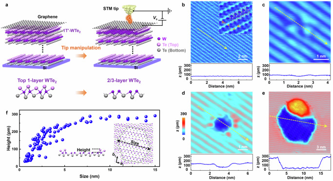
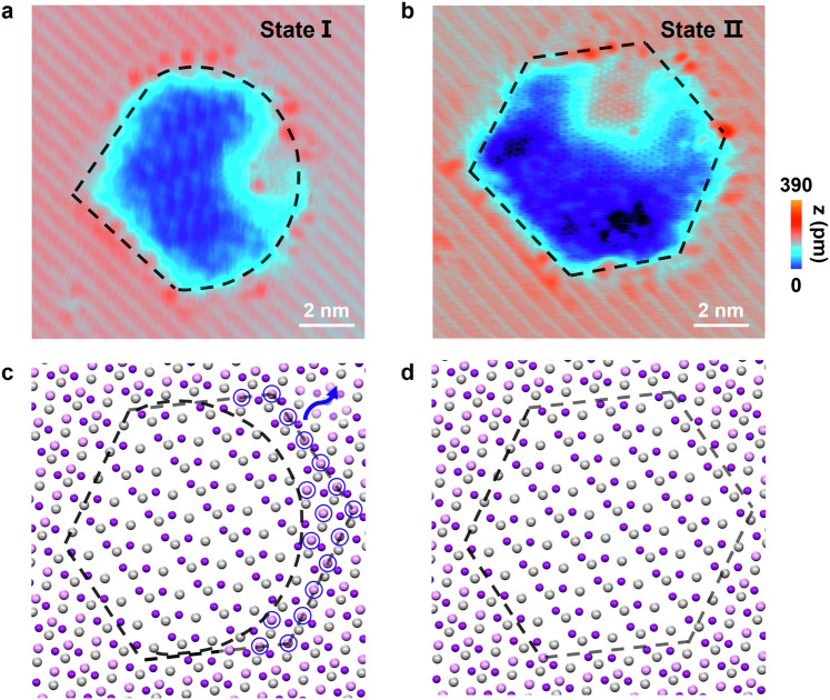
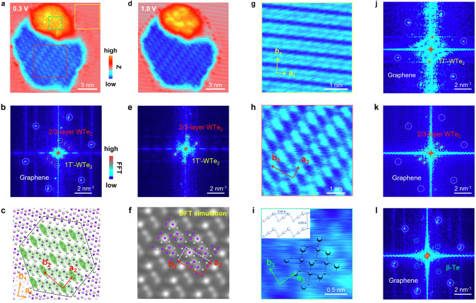
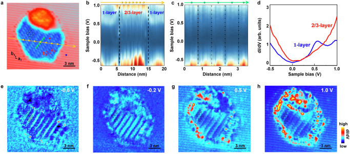
Layered van der Waals transition metal dichalcogenides (TMDCs), generally composed of three atomic X-M-X planes in each layer (M = transition metal, X = chalcogen), provide versatile platforms for exploring diverse quantum phenomena. In each MX2 layer, the M-X bonds are predominantly covalent in nature and, as a result, the cleavage of TMDC crystals normally occurs between the layers. Here we report the controllable realization of fractional-layer WTe2 via an in-situ scanning tunneling microscopy (STM) tip manipulation technique. By applying STM tip pulses, hundreds of the topmost Te atoms are removed to form a nanoscale monolayer Te pit in the 1 T'-WTe2, thus realizing a 2/3-layer WTe2 film. Such a configuration undergoes a spontaneous atomic reconstruction, yielding a unidirectional charge density redistribution with the wavevector and geometry quite distinct from that of pristine 1 T'-WTe2. Our results expand the conventional understanding of the TMDCs and are expected to stimulate further research on the structure and properties of fractional-layer TMDCs.


Conflict of interest statement

Competing interests: The authors declare no competing interests.

Figures

Fig. 1
Fig. 1. Nanoscale fabrication of 2/3-layer WTe2.
a Schematic of fabricating 2/3-layer WTe2. Upper panel: Experimental set-up. 1 T′-WTe2 crystal is firstly placed onto Si substrates, and then covered by graphene monolayer. The 2/3-layer WTe2 can be realized by applying a scanning tunneling microscopy (STM) tip pulse. Bottom panel: The 2/3-layer WTe2 is derived from its monolayer by removing the topmost Te atoms. b Upper panel: large-scale STM image of graphene-covered 1 T′-WTe2 before applying a STM tip pulse. STM parameters: Vs = 1 V (bias voltage with respect to the sample), I = 100 pA (tunneling current). Inset: atomically resolved STM image (Vs = 1 V, I = 100 pA). Bottom panel: height profile recorded along the yellow arrow. ce Upper panels: STM images after applying a STM tip pulse of 3 V, 4 V, and 8 V for 10 ms duration, respectively (Vs = 1 V, I = 100 pA). Bottom panels: height profiles recorded along the yellow arrows. f The depth of the pit as a function of its lateral size. Inset: Top and side views of the atomic structure of 2/3-layer WTe2 embedded into 1 T′-WTe2. The depth and the lateral size of the pit are marked.
Fig. 2
Fig. 2. STM verification for realizing fractional-layer 1 T′-WTe2.
a STM image of graphene-covered 1 T′-WTe2 after applying a STM tip pulse of 6 V for 10 ms duration. The pit shows an irregular hexagonal outline (Vs = 1 V, I = 100 pA). b Typical STM image after applying an additional STM tip pulse of 4 V for 70 ms duration (Vs = 1 V, I = 100 pA). The pit becomes a regular hexagon. c, d Schematic of the formation process of 2/3-layer WTe2. The arrow in panel (c) symbolically shows that the marked atoms are released. The outlines of the pits in panels (ad) are marked by the dashed lines.
Fig. 3
Fig. 3. Atomically resolved STM images around the tip-induced pit.
a, d Typical STM images of graphene-covered 1 T′-WTe2 after applying a tip pulse of 8 V for 10 ms duration under the sample biases of 0.3 V and 1.0 V (I = 100 pA). The sizes of the images are 16 × 16 nm2 and the resolutions are 320 × 320 pixels. The regions of graphene-covered 1 T′-WTe2, 2/3-layer WTe2, and β-Te are marked by the yellow, red, and green dashed boxes, respectively. b, e, Fourier transforms of panels a and d by using the square root normalization. The bright spots marked by the white, yellow, and red circles indicate the reciprocal lattices of graphene, 1 T′-WTe2, and 2/3-layer WTe2. c Model of atomically reconstructed 2/3-layer WTe2, where a2 = a1 + b1, b2 = −3a1 + b1. f DFT calculation of the atomic structure and the corresponding STM simulation of the relaxed 2/3-layer WTe2. gi High-resolution STM images of graphene-covered 1 T′-WTe2, 2/3-layer WTe2, and β-Te recorded at the regions marked in panel a by the yellow, red, and green dashed boxes (Vs = 1 V, I = 100 pA). The sizes of the images are 4 × 4 nm2, 6 × 6 nm2, 3 × 3 nm2, and the resolutions are 320 × 320 pixels. The measured superlattice constants of 2/3-layer WTe2 are a2 = 8.2 Å, b2 = 13.7 Å with the intersection angle of 86°, and the rotated angle between a2 and a1 is 63°. jl Fourier transforms of panels g-i by using the square root normalization.
Fig. 4
Fig. 4. Electronic properties of 2/3-layer WTe2.
a STM image of graphene-covered 1 T′-WTe2 after applying a STM tip pulse of 8 V for 10 ms duration (Vs = 1 V, I = 100 pA). b, c Site-dependent scanning tunneling spectroscopy (STS) spectra recorded along the yellow and green arrows marked in panel a. The edges of the 2/3-layer WTe2 are marked by the black dashed lines. d STS spectra acquired at the locations marked in panel a. The blue and red lines correspond to the STS spectra recorded on graphene-covered 1 T′-WTe2 and 2/3-layer WTe2, respectively. e–h Spectroscopic maps acquired at the same location as panel a under the sample bias of −0.6, −0.2, 0.5, and 1.0 eV, respectively.

Similar articles

References

    1. Manzeli, S., Ovchinnikov, D., Pasquier, D., Yazyev, O. V. & Kis, A. 2D transition metal dichalcogenides. Nat. Rev. Mater.2, 17033 (2017).
    1. Liu, G., Xiao, D., Yao, Y., Xu, X. & Yao, W. Electronic structures and theoretical modelling of two-dimensional group-VIB transition metal dichalcogenides. Chem. Soc. Rev.44, 2643 (2015). - PubMed
    1. Zhou, J. et al. A library of atomically thin metal chalcogenides. Nature556, 355 (2018). - PubMed
    1. Liu, C. et al. Two-dimensional materials for next-generation computing technologies. Nat. Nanotechnol.15, 545–557 (2020). - PubMed
    1. Gentile, P. et al. Electronic materials with nanoscale curved geometries. Nat. Electron.5, 551–563 (2022).

LinkOut - more resources