

1.3 Micron Photodetectors Enabled by the SPARK Effect
- PMID: 40283315
- PMCID: PMC12029151
- DOI: 10.3390/mi16040440
1.3 Micron Photodetectors Enabled by the SPARK Effect
Abstract
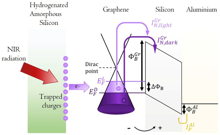
In this work, we present a graphene-based photodetector operating at a wavelength of 1310 nm. The device leverages the SPARK effect, which has previously been investigated only at 1550 nm. It features a hybrid waveguide structure comprising hydrogenated amorphous silicon, graphene, and crystalline silicon. Upon optical illumination, defect states release charge carriers into the graphene layer, modulating the thermionic current across the graphene/crystalline silicon Schottky junction. The photodetector demonstrates a peak responsivity of 0.3 A/W at 1310 nm, corresponding to a noise-equivalent power of 0.4 pW/Hz1/2. The experimental results provide deeper insights into the SPARK effect by enabling the determination of the efficiency × lifetime product of carriers at 1310 nm and its comparison with values previously reported at 1550 nm. The wavelength dependence of this product is analyzed and discussed. Additionally, the response times of the device are measured and evaluated. The silicon-based fabrication approach employed is versatile and does not rely on sub-micron lithography techniques. Notably, reducing the incident optical power enhances the responsivity, making this photodetector highly suitable for power monitoring applications in integrated photonic circuits.
Keywords: graphene; near-infrared; photodetectors; silicon; waveguide.
Conflict of interest statement
The authors declare no conflicts of interest.
Figures


References
-
- Jalali B., Fathpour S. Silicon Photonics. J. Light. Technol. 2006;24:4600–4615. doi: 10.1109/JLT.2006.885782. - DOI
-
- Soref R. The Past, Present, and Future of Silicon Photonics. IEEE J. Sel. Top. Quantum Electron. 2007;12:1678–1687. doi: 10.1109/JSTQE.2006.883151. - DOI
-
- Reed G.T. Silicon Photonics: The State of the Art. John Wiley & Sons; Hoboken, NJ, USA: 2008. [(accessed on 1 February 2025)]. Available online: https://books.google.it/books?hl=it&lr=&id=NVmnuGREwj4C&oi=fnd&pg=PR7&dq....
-
- Thomson D., Zilkie A., Bowers J.E., Komljenovic T., Reed G.T., Vivien L., Marris-Morini D., Cassan E., Virot L., Fédéli J.M., et al. Roadmap on Silicon Photonics. J. Opt. 2016;18:073003. doi: 10.1088/2040-8978/18/7/073003. - DOI
-
- Li C., Guo P., Xie S.W., Luo L.W., Siew S.Y., Luo X., Dong B., Zheng H.Y., Zhang W., Gao F., et al. Review of Silicon Photonics Technology and Platform Development. J. Light. Technol. 2021;39:4374–4389. doi: 10.1109/JLT.2021.3066203. - DOI
Grants and funding
LinkOut - more resources
Full Text Sources
