Review
. 2025 Apr 11;16(4):453.
doi: 10.3390/mi16040453.

A Review on AC-Dielectrophoresis of Nanoparticles

Affiliations
Review

A Review on AC-Dielectrophoresis of Nanoparticles

Tonoy K Mondal et al. Micromachines (Basel). .

Abstract

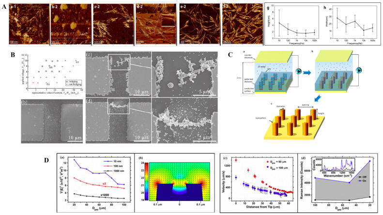
Dielectrophoresis at the nanoscale has gained significant attention in recent years as a low-cost, rapid, efficient, and label-free technique. This method holds great promise for various interdisciplinary applications related to micro- and nanoscience, including biosensors, microfluidics, and nanomachines. The innovation and development of such devices and platforms could promote wider applications in the field of nanotechnology. This review aims to provide an overview of recent developments and applications of nanoparticle dielectrophoresis, where at least one dimension of the geometry or the particles being manipulated is equal to or less than 100 nm. By offering a theoretical foundation to understand the processes and challenges that occur at the nanoscale-such as the need for high field gradients-this article presents a comprehensive overview of the advancements and applications of nanoparticle dielectrophoresis platforms over the past 15 years. This period has been characterized by significant progress, as well as persistent challenges in the manipulation and separation of nanoscale objects. As a foundation for future research, this review will help researchers explore new avenues and potential applications across various fields.

Keywords: colloids; dielectrophoresis; microelectrodes; microfluidics; nanoelectrodes; nanomanipulation; nanoparticles.


Conflict of interest statement

The authors declare no conflicts of interest.

Figures

Figure 1
Figure 1
The number of papers published in nanoparticles DEP field over time. The data came from an open-source, date-restricted Web of Science search for “dielectrophoresis” and “nanoparticles”. After 2010, the number of yearly publications has remained largely unchanged.
Figure 2
Figure 2
(A) Effect of frequency on nanoribbons development with applied frequency of (a-1) 100 Hz, (b-2) 1 kHz, (c-2) 10 kHz, (d-2) 100 KHz, (e-2) 1 MHz, (f-2) 10 MHz, (g) the distribution of height with frequency, and (h) the distribution of width with frequency [91]; (B) Au nanoparticle chain formation with 10 μm-wide gap: (a) formation condition plot between applied voltage (Vgap) and representative value of current, SEM image in the case of (b) 2.0 Vrms with 4.9 mArms, (c) 10.0 Vrms with 60 mArms, and (d) 8.1 Vrms with 6.4 mArms. Adapted and modified with permission from [93]. Copyright 2017 John Wiley and Sons. (C) Electric field-directed assembly of NPs towards fabricating 3D nanostructures: (a,b) NPs suspended in aqueous solution are (a) assembled and (b) fused in the pattern via geometries under an applied AC electric field, (c) removal of the patterned insulator film after the assembly. Adapted and modified with permission from [73]. Copyright 2014 American Chemical Society. (D) Influence of device configuration on trapping and SERS enhancement: (a) gradient of electric field-squared as a function of electrode separation, (b) gradient of field-squared logarithmic colormap, (c) particle tracking of AuNP at two different gaps, and (d) SERS measurement with and without DEP trapping. Adapted and modified with permission from [94]. Copyright 2016 American Chemical Society.
Figure 3
Figure 3
(A) Fluorescence images of polystyrene (PS) particles (a) without AC fields. With 10 VPP and an AC frequency of (b) 1 MHz, (c) 5 MHz, (d) 7 MHz, and (e) 10 MHz. Adapted with permission from [72]. Copyright 2010 American Chemical Society. (B) (a) Illustration of the experiment for DEP concentration of analyte molecules. (b) Simulation of the electric field intensity gradient. (c) SEM of the nanohole array [112]. (C) Fabrication of gold pyramid, its connection to tungsten wire and SEM images of gold pyramids in the mold and a single pyramid [113]. (D) DEP trapping by conductive nanofiber mat: 1 µm PS particles (a) without AC fields, (b) with AC fields, and (c) SEM image; 210 nm PS particles (d) without AC fields, (e) with AC fields, and (h) SEM image; 20 nm PS particles (f) without AC fields, and (g) with AC fields. Adapted from [86] with permission from The Royal Society of Chemistry. (E) DEP trapping of 30 nm PS beads with very-low AC fields. (a) Illustration of nanogap electrodes array for DEP trapping. (b) Fluorescence image of PS beads trapped across three 20 μm nanogaps. (c,d) SEM images of DEP trapping of PS beads along the nanogap. Adapted and modified from [114]. Figure 3B,C,E are an unofficial adaptation of articles that appeared in an ACS publication. ACS has not endorsed the content of this adaptation or the context of its use.
Figure 4
Figure 4
(A) Mean electrode connection yield (with 1 SD as error bar) after DEP of CNTs dispersed in cyclohexanone, water, and IPA solution: applied voltage was 2 VTOT with 2 µm of oxide layer. Adapted with permission from [142]. Copyright 2010 American Chemical Society. (B) Design of a self-limiting dielectrophoretic device featuring a microscopic image of an array with four units, each consisting of a pair of trapping electrodes connected in series with a capacitor. Adapted and modified with permission from [143]. Copyright 2022 American Chemical Society. (C) Schematic of patterning technique by SSAW (a) randomly dispersed NWs, (b) 1D-, (c) 2D-SSAW fields formed NW arrays, (d) assembled into bundles due to E. field, and (e) observed 3D-sparked at the nodes. Adapted and modified with permission from [144]. Copyright 2013 American Chemical Society. (D) (a) Schematic diagram of Pt-Au catalytic nanomotors manipulations with AC electric fields, (b) SEM image, (c) energy-dispersive X-ray spectroscopy images of catalytic nanomotors, and (d) snapshots of a nanomotor manipulation. Adapted with permission from [145]. Copyright 2018 American Chemical Society.
Figure 5
Figure 5
(A) (a) Optical, (b) higher magnification optical microscopy image of the patterned electrode, (c) experimental setup schematic, and (d) schematic showing assembled GO nanostructures and Pt NPs. Adapted with permission from [164]. Copyright 2015 American Chemical Society. (B) (a,b) SEM image of DEP electrodes: zoomed in view of the electrode gap (b) marked by the dotted white circle in (a), (c) schematic of the experimental setup used for DEP, (d) TEM image of the 50 μL CdTe NPs dispersion after DEP. Adapted with permission from [166]. Copyright 2011 American Chemical Society. (C) Orientation of nanorod LEDs schematic when aligned: (a) cross-sectional and (b) top-view images of nanorod alignment using an AC electric field, and (c) randomly aligned and with DC voltage approximately half of them turned on; (d) cross-sectional and (e) top-view images of nanorod LED device using AC electric field with DC offset. Most of them were forwardly aligned due to the intrinsic dipole torque and (f) the aligned LEDs were mostly turned on when DC voltage was applied. Adapted with permission from [167]. Copyright 2017 American Chemical Society.

References

    1. Li F., Josephson D.P., Stein A. Colloidal assembly: The road from particles to colloidal molecules and crystals. Angew. Chem. Int. Ed. 2011;50:360–388. doi: 10.1002/anie.201001451. - DOI - PubMed
    1. Velev O.D., Gupta S. Materials fabricated by micro-and nanoparticle assembly–the challenging path from science to engineering. Adv. Mater. 2009;21:1897–1905. doi: 10.1002/adma.200801837. - DOI
    1. Arpin K.A., Mihi A., Johnson H.T., Baca A.J., Rogers J.A., Lewis J.A., Braun P.V. Multidimensional architectures for functional optical devices. Adv. Mater. 2010;22:1084–1101. doi: 10.1002/adma.200904096. - DOI - PubMed
    1. Dies H., Raveendran J., Escobedo C., Docoslis A. In situ assembly of active surface-enhanced Raman scattering substrates via electric field-guided growth of dendritic nanoparticle structures. Nanoscale. 2017;9:7847–7857. doi: 10.1039/C7NR01743J. - DOI - PubMed
    1. Rozynek Z., Han M., Dutka F., Garstecki P., Józefczak A., Luijten E. Formation of printable granular and colloidal chains through capillary effects and dielectrophoresis. Nat. Commun. 2017;8:15255. doi: 10.1038/ncomms15255. - DOI - PMC - PubMed

LinkOut - more resources