

Enhanced photoresponse in a Ag2S/In2Se3 heterojunction based visible light photodetector
- PMID: 40330035
- PMCID: PMC12053964
- DOI: 10.1039/d5ra00917k
Enhanced photoresponse in a Ag2S/In2Se3 heterojunction based visible light photodetector
Abstract
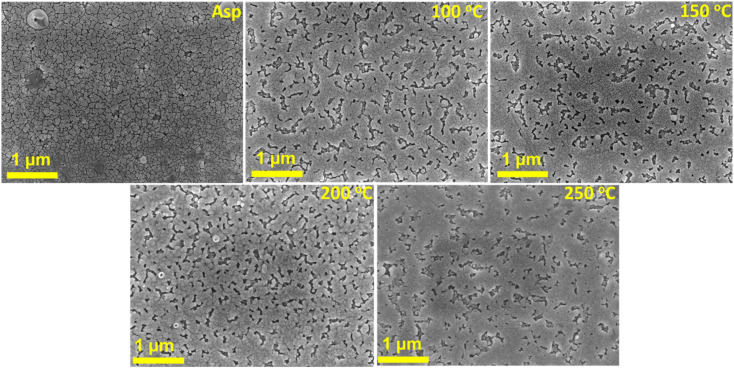
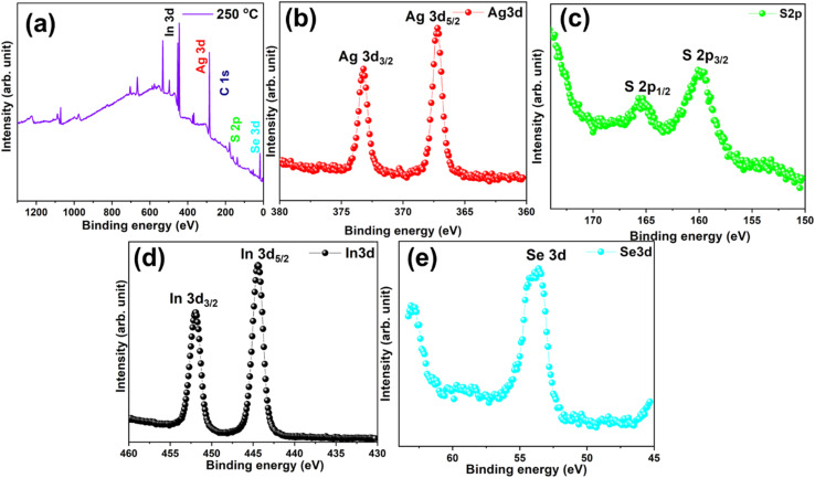
Ag2S and In2Se3, two prominent functional materials, have recently gained extensive research attention. Ag2S shows good chemical stability with excellent photoconducting ability as a direct, narrow band-gap semiconductor. In2Se3 compounds have been widely used in optoelectronics, photodetectors, and gas sensors. In this work, we develop a visible light photodetector by combining these two materials from Ag2S/In2Se3 heterostructure films at room temperature. The Ag2S/In2Se3 bilayer films were annealed at different temperatures, and their photodetection parameters were compared to different annealed films. The bilayer structure and the interdiffusion of Ag2S into the In2Se3 layer were confirmed through a cross-sectional FESEM view. The 250 °C annealed sample shows better photoconductivity with a maximum responsivity of 2.01 × 10⁻¹ A/W and 7.32 × 10⁹ Jones of detectivity than the other films. The current increase from nA to mA upon annealing significantly increased the photo response of the 250 °C annealed films. The hydrophilic properties improved with annealing, as confirmed by contact angle measurement. It is also further verified by the increased porosity observed from the FESEM images of the surface morphology. The transition from amorphous to polycrystalline was confirmed through XRD. The interdiffusion by annealing resulted in the formation of ternary phases like AgInS2 and AgInSe2, as seen from the XRD and HRTEM data. The crystallite size that increased upon annealing reduced the dislocation density from 3.29 × 10¹⁵ to 2.73 × 10¹⁵ m-2. The optical bandgap, density, extinction coefficient, and skin depth showed changes as probed by UV-visible spectroscopy. Upon annealing, the band gap was enhanced by 0.157 eV from its as-prepared state. The observed changes in optical parameters and photoconductivity make the film a suitable candidate for visible light photodetection.
This journal is © The Royal Society of Chemistry.
Conflict of interest statement
There are no conflicts to declare.
Figures


References
-
- Khan M. Bhatti K. A. Qindeel R. Aleem F. Rehman N. Alonizan N. Sol-gel deposition and characterization of multilayer 2% Cu doped TiO2 nanostructured thin films. J. Mater. Sci.:Mater. Electron. 2017;28:9471–9477. doi: 10.1007/s10854-017-6690-3. - DOI
-
- Khan M. I. Imran S. Shahnawaz Saleem M. Rehman S. U. Annealing effect on the structural, morphological and electrical properties of TiO2/ZnO bilayer thin films. Results Phys. 2018;8:249–252. doi: 10.1016/j.rinp.2017.12.030. - DOI
-
- Kim J. Barmak K. Graef M. D. Lewis L. H. Crew D. C. Effect of annealing on magnetic exchange coupling in CoPt/Co bilayer thin films. J. Appl. Phys. 2000;87:6140–6142. doi: 10.1063/1.372635. - DOI
-
- Tani J. I. Ishikawa H. Fabrication and analysis of Mg3Bi2 thin films by post-annealing Mg/Bi bilayer thin films. Mater. Lett. 2023;331:133460. doi: 10.1016/j.matlet.2022.133460. - DOI
-
- Yadav R. K. Pawar P. S. Kim Y. T. Sharma I. Patil P. R. Bisht N. Heo J. Investigation of hybrid SnSe/SnS bilayer absorber for application in solar cells. Sol. Energy. 2023;266:112274. doi: 10.1016/j.solener.2023.112174. - DOI
LinkOut - more resources
Full Text Sources
Miscellaneous