

Diamond thin films: a twenty-first century material. Part 2: a new hope
- PMID: 40336287
- PMCID: PMC12059586
- DOI: 10.1098/rsta.2023.0382
Diamond thin films: a twenty-first century material. Part 2: a new hope
Abstract
Nearly a quarter of a century ago, we wrote a review paper about the very new technology of chemical vapour deposition (CVD) of diamond thin films. We now update this review and bring the story up to date by describing the progress made-or not made-over the intervening years. Back in the 1990s and early 2000s, there was enormous excitement about the plethora of applications that were suddenly possible now that diamonds could be fabricated in the form of thin films. Diamond was hailed as the ultimate semiconductor, and it was believed that the few remaining problems would be quickly solved, leading to a new 'diamond age' of electronics. In reality, however, difficulty in making large-area diamond wafers and the elusiveness of a useful n-type dopant slowed progress substantially. Unsurprisingly, over the following decade, the enthusiasm and funding for diamonds faded, while competing materials forged ahead. But in the early 2010s, several new game-changing applications for diamonds were discovered, such as electrochemical electrodes, the nitrogen-vacancy (NV) centre defect that promised room-temperature quantum computers, and methods to grow large single-crystal gemstone-quality diamonds. These led to a resurgence in diamond research and a new hope that diamond might finally live up to its promise.This article is part of the theme issue 'Science into the next millennium: 25 years on'.
Keywords: chemical vapour deposition; diamond; review.
Conflict of interest statement
We declare we have no competing interests.
Figures

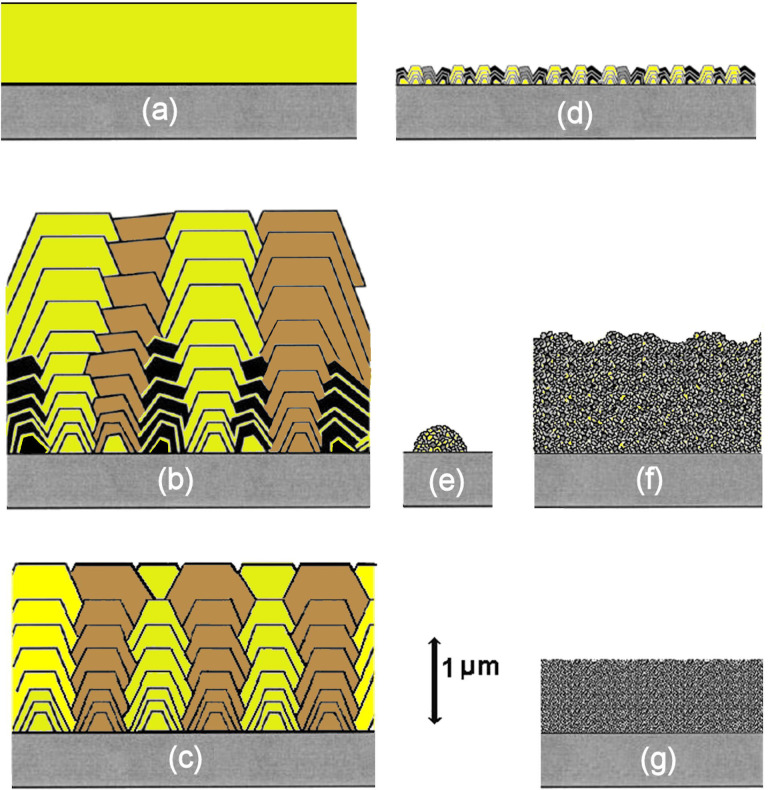
![(a) Schematic diagram of a DAAM system, redrawn from [22].](https://cdn.ncbi.nlm.nih.gov/pmc/blobs/156a/12059586/b293eeca4216/rsta.2023.0382.f002.jpg)


References
-
- May PW. 2000. Diamond thin films: a 21st-century material. Phil.Trans. R. Soc. Lond. A 358, 473–495. ( 10.1098/rsta.2000.0542) - DOI
-
- Onstad E, Clarke D. 2018. How man-made diamonds have grown to threaten natural gems. Reuters Business News. See https://www.reuters.com/article/idUSKCN1OK0N4/ (accessed 7 March 2024).
-
- Nebel CE. 2023. CVD diamond: a review on options and reality. Funct. Diam. 3, 2201592. ( 10.1080/26941112.2023.2201592) - DOI
-
- Zulkharnay R, May PW. 2024. Applications of diamond films: a review. Funct. Diam 4, 2410160. ( 10.1080/26941112.2024.2410160) - DOI
Publication types
Grants and funding
LinkOut - more resources
Full Text Sources