

Colloidal CuInS2 quantum well nanostructures with II-VI semiconductors as barrier layers
- PMID: 40342912
- PMCID: PMC12056669
- DOI: 10.1039/d5sc00657k
Colloidal CuInS2 quantum well nanostructures with II-VI semiconductors as barrier layers
Abstract
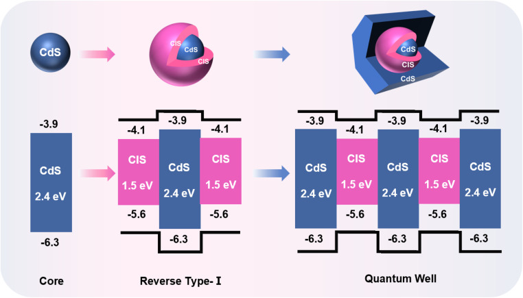
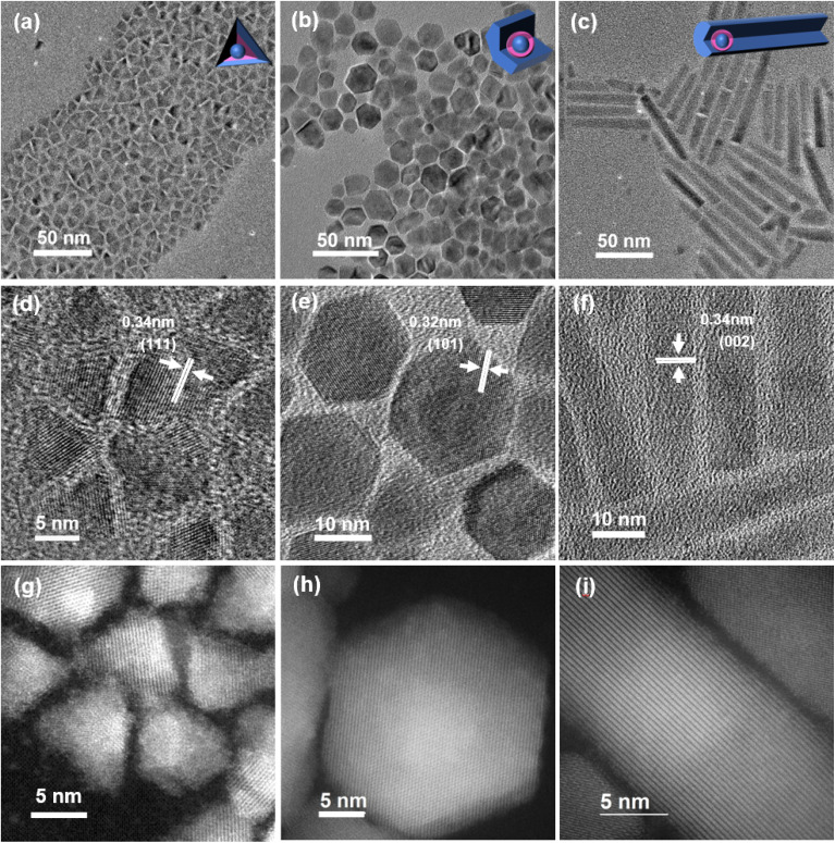
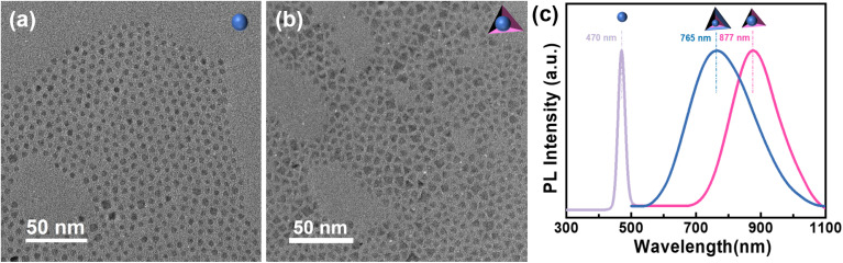
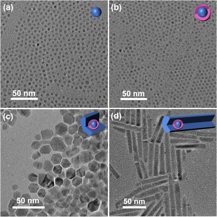
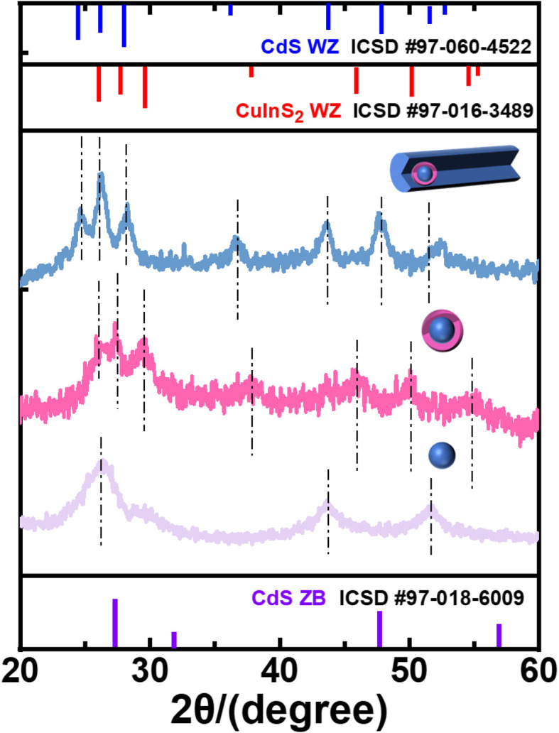
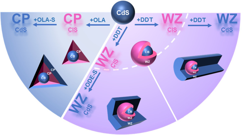
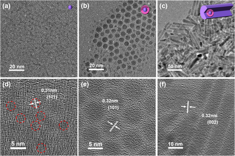
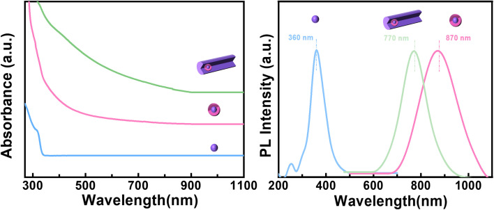
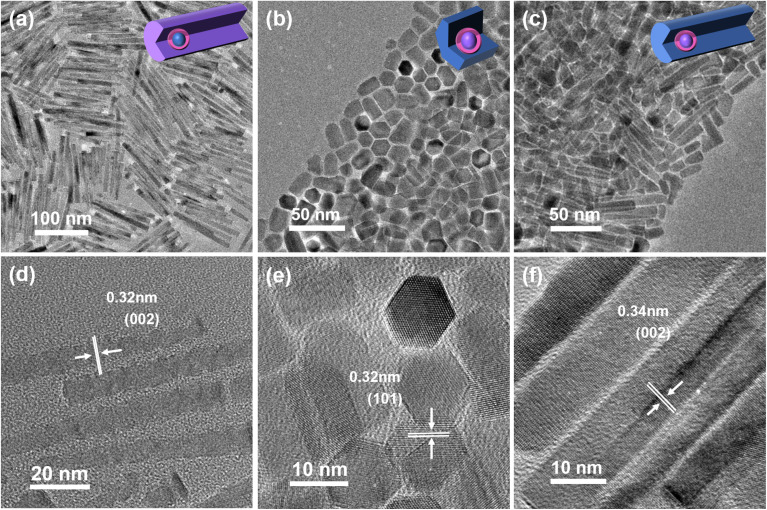
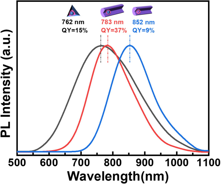
Quantum well (QW) structures have been successfully produced and utilized in high-performance optoelectronic devices. By designing QW structures at the nanoscale, it is possible to combine the advantages of both QW structures and nanostructures, resulting in extraordinary properties. In this study, a CuInS2 (CIS) quantum well layer was successfully constructed within a single nanostructure using a colloidal method. Various QW nanostructures were synthesized, including CdS/CIS/CdS, CdS/CIS/ZnS, ZnS/CIS/CdS, and Cd-free ZnS/CIS/ZnS configurations. The shapes of these QW nanostructures were precisely tuned to form tetrahedrons, hexagonal columns, and rods. Importantly, the morphology and crystal structure of the CIS layer play a crucial role in determining the final morphologies of the QW nanostructures. These QW nanostructures exhibit fluorescence emission in the near-infrared range (NIR), achieving a maximum quantum yield of 37% at 783 nm. This work demonstrates the successful construction of a CIS quantum well layer within a single colloidal nanoparticle, providing a valuable research model for fundamental studies and offering promising materials for optoelectronic devices.
This journal is © The Royal Society of Chemistry.
Conflict of interest statement
The authors declare no conflict of interest.
Figures
Similar articles
-
Solution-processed, barrier-confined, and 1D nanostructure supported quasi-quantum well with large photoluminescence enhancement.ACS Nano. 2014 Apr 22;8(4):3771-80. doi: 10.1021/nn500465w. Epub 2014 Mar 6. ACS Nano. 2014. PMID: 24580094
-
Highly Luminescent Water-Dispersible NIR-Emitting Wurtzite CuInS2/ZnS Core/Shell Colloidal Quantum Dots.Chem Mater. 2017 Jun 13;29(11):4940-4951. doi: 10.1021/acs.chemmater.7b01258. Epub 2017 May 22. Chem Mater. 2017. PMID: 28638177 Free PMC article.
-
Rigid CuInS2/ZnS Core/Shell Quantum Dots for High Performance Infrared Light-Emitting Diodes.Nano Lett. 2024 May 1;24(17):5342-5350. doi: 10.1021/acs.nanolett.4c01249. Epub 2024 Apr 17. Nano Lett. 2024. PMID: 38630899
-
Syntheses and applications of Mn-doped II-VI semiconductor nanocrystals.J Nanosci Nanotechnol. 2005 Sep;5(9):1364-75. doi: 10.1166/jnn.2005.308. J Nanosci Nanotechnol. 2005. PMID: 16193951 Review.
-
64Cu-1,4,7,10-Tetraazacyclododecane-1,4,7,10-tetraacetic acid-quantum dot-vascular endothelial growth factor.2008 Jul 1 [updated 2008 Aug 12]. In: Molecular Imaging and Contrast Agent Database (MICAD) [Internet]. Bethesda (MD): National Center for Biotechnology Information (US); 2004–2013. 2008 Jul 1 [updated 2008 Aug 12]. In: Molecular Imaging and Contrast Agent Database (MICAD) [Internet]. Bethesda (MD): National Center for Biotechnology Information (US); 2004–2013. PMID: 20641777 Free Books & Documents. Review.
References
-
- Mata M. d. l. Zhou X. Furtmayr F. Teubert J. Gradečak S. Eickhoff M. Fontcuberta i Morral A. Arbiol J. A review of MBE grown 0D, 1D and 2D quantum structures in a nanowire. J. Mater. Chem. C. 2013;1:4300–4312. doi: 10.1039/C3TC30556B. - DOI
-
- Haynes C. L. Duyne R. P. V. Nanosphere Lithography: A Versatile Nanofabrication Tool for Studies of Size-Dependent Nanoparticle Optics. J. Phys. Chem. B. 2001;105:5599–5611. doi: 10.1021/jp010657m. - DOI
LinkOut - more resources
Full Text Sources
Miscellaneous