. 2025 May 16;11(20):eadu3840.
doi: 10.1126/sciadv.adu3840. Epub 2025 May 14.

Pixelation of perovskite quantum wire thin films with 0.18-μm features and 63,500-ppi pixel density

Affiliations

Pixelation of perovskite quantum wire thin films with 0.18-μm features and 63,500-ppi pixel density

Qianpeng Zhang et al. Sci Adv. .

Abstract

Halide perovskite materials excel in broad optoelectronic applications, and there is an urgent demand to develop perovskite-based integrated optoelectronic devices. However, the limitations posed by the incompatibility of perovskite thin film with wet lithography greatly hinder its potential in many important applications, including ultrahigh-density displays, high-resolution image sensors, high-density memristors, and integrated photonic circuitry. To tackle this bottleneck problem, we develop the self-aligned close-spaced sublimation growth of perovskite quantum wires and demonstrate 0.18-micrometer feature size perovskite patterns, meanwhile achieving a pixel density of 63,500 pixels per inch, the highest reported for perovskite. We showcase pixelation of perovskite quantum wires with color conversion films, addressing the need for full-color microdisplays. In addition, we demonstrate these films on curved substrates, holding promise for near-eye microdisplays. Processes shown here can also apply to other perovskite devices such as high-resolution displays, image sensing, and memristor arrays.


Figures

Fig. 1.
Fig. 1.. Mechanism of sa-CSS growth of perovskite quantum wires and different pixelation processes.
(A) Mechanism diagram of the sa-CSS method. The PAM enables self-aligned growth in specific areas. (B) Diagram of the pixelation process flow using photolithography and RIE. (C) Diagram of the pixelation process flow using EBL for ultrahigh resolution. The PMMA layer is lifted up in the image to show the quantum wires (QWRs) in the PAM but is not necessarily removed during the experiment. (D) Diagram of the perovskite (PRK) quantum wire growth process flow on nonplanar (e.g., hemispherical) substrate. Quantum wires can grow on either the convex side (option 1) or the concave side (option 2).
Fig. 2.
Fig. 2.. Mechanisms for sa-CSS growth of perovskite quantum wires and the calculation results from first-principles theory and molecular dynamics method.
(A) Adsorption of CsPbBr3 on the Al2O3 surface and the (B) absorption energy at different adsorption sites (results from first-principles theory calculations). (C) Pb atom counts per unit distance for different pore sizes. (D) Adsorption processes of CsPbBr3 with varying pore sizes (results from molecular dynamics method calculations).
Fig. 3.
Fig. 3.. Perovskite quantum wire thin film as color conversion film.
(A) CIE 1931 plot from the PL spectra in (G) to (I), and the color gamut is 87.7%. R, red; B, blue; G, green. (B) Red color film grown with solution method. (C) Change of the film color by controlling the pore size of the PAM. Green and blue films are from CsPbBr3 quantum wires with pore size of 5.7 and 2.66 nm, respectively, giving PL peaks of 519 and 482 nm, respectively. (D) PL spectra of CsPbBr3 quantum wires with ALD of 0/5/10 cycles. (E) Bandgap shift versus the 1/d2, where d is the diameter of the quantum wires. (F) XRD spectrum of the CsPbBr3 quantum wires grown in PAM on FTO substrate. (110) and (200) peaks are from perovskite, and peaks marked with asterisk are from SnO2. (G to I) PL spectra of red, green, and blue quantum wire films with excitation light source spectra for PLQY measurement. Emission peaks for red, green, and blue are 677, 510, and 482 nm, respectively, with corresponding PLQYs of 24.63, 33.35, and 37.07%, respectively.
Fig. 4.
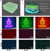
Fig. 4.. Demonstration of the color conversion from a UVA microdisplay panel.
(A) Diagram of the perovskite quantum wire arrays. (B) Diagram of the color conversion demonstration set up. From bottom to top are drive circuitry, GaInN micro-LED arrays, perovskite quantum wires in PAM, and blue/UV color filter. The color filter filters away light with wavelength less than 500 nm. (C) UVA panel showing a HKUST logo. The size of the white square dashed lines is 1.95 mm by 1.98 mm. Images converted to (D) green and (E) red colors. (F to H) Red and (I to K) green pixel arrays with pitches of [(F) and (I)] 10 μm, [(G) and (J)] 20 μm, and [(H) and (K)] 30 μm, corresponding to pixel densities of 2540, 1270, and 847 ppi, respectively.
Fig. 5.
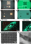
Fig. 5.. Pixelation results with EBL.
The QR patterns with different sizes are shown. (A) Optical photo and (B) photo under UV light of QR codes with different sizes: 17 μm by 17 μm, 34 μm by 34 μm, 68 μm by 68 μm, 136 μm by 136 μm, and 272 μm by 272 μm. (C) Optical photo and (D) photo under UV light of the zoomed-in area indicated with red rectangular in (A). The QR patterns link to the website of our research group. (E) Milky Way Galaxy demonstration of the pixelation with feature size down to 0.18 μm. (F) SEM image of circular arrays with a pitch size of 400 nm, corresponding to a pixel density of 63,500 ppi. (G) Transmission electron microscopy (TEM) image of a single CsPbBr3 quantum wire.
Fig. 6.
Fig. 6.. Hemispherical color conversion film for potential contact lens microdisplay application.
(A) Diagram showing the concept of the color conversion film for contact lens microdisplay. (B) A prototype hemispherical film with potential application as a contact lens. Note that the sample does not touch human eye and is just for concept proof. (C) Convex side and (D) concave side of the green perovskite quantum wire–based color conversion film. (E) Convex side and (F) concave side of the red perovskite quantum wire–based color conversion film. (G) Diagram showing the testing setup: UVA display panel/hemispherical transparent substrate/hemispherical color conversion film/color filter. (H) Optical photo of a working UVA/hemispherical color conversion film architecture. (I) Optical photo of a working UVA/hemispherical color conversion film/color filter architecture.

Similar articles

References

    1. Gu L., Poddar S., Lin Y., Long Z., Zhang D., Zhang Q., Shu L., Qiu X., Kam M., Javey A., Fan Z., A biomimetic eye with a hemispherical perovskite nanowire array retina. Nature 581, 278–282 (2020). - PubMed
    1. Wang W.-T., Holzhey P., Zhou N., Zhang Q., Zhou S., Duijnstee E. A., Rietwyk K. J., Lin J.-Y., Mu Y., Zhang Y., Bach U., Wu C.-G., Yip H. L., Snaith H. J., Feng S.-P., Water- and heat-activated dynamic passivation for perovskite photovoltaics. Nature 632, 294–300 (2024). - PMC - PubMed
    1. Zhou Y., Sun Z., Ding Y., Yuan Z., Qiu X., Cao Y. B., Wan Z., Long Z., Poddar S., Kumar S., Ye W., Chan C. L. J., Zhang D., Ren B., Zhang Q., Kwok H.-S., Li M. G., Fan Z., An ultrawide field-of-view pinhole compound eye using hemispherical nanowire array for robot vision. Sci. Robot. 9, eadi8666 (2024). - PubMed
    1. Zhang Q., Tavakoli M. M., Gu L., Zhang D., Tang L., Gao Y., Guo J., Lin Y., Leung S.-F., Poddar S., Fu Y., Fan Z., Efficient metal halide perovskite light-emitting diodes with significantly improved light extraction on nanophotonic substrates. Nat. Commun. 10, 727 (2019). - PMC - PubMed
    1. Gallop N. P., Maslennikov D. R., Mondal N., Goetz K. P., Dai Z., Schankler A. M., Sung W., Nihonyanagi S., Tahara T., Bodnarchuk M. I., Kovalenko M. V., Vaynzof Y., Rappe A. M., Bakulin A. A., Ultrafast vibrational control of organohalide perovskite optoelectronic devices using vibrationally promoted electronic resonance. Nat. Mater. 23, 88–94 (2024). - PMC - PubMed

LinkOut - more resources