. 2025 Aug;37(32):e2501821.
doi: 10.1002/adma.202501821. Epub 2025 May 21.

Flexible Selenium Nanowires with Tuneable Electronic Bandgaps

Affiliations

Flexible Selenium Nanowires with Tuneable Electronic Bandgaps

William J Cull et al. Adv Mater. 2025 Aug.

Abstract

Manipulating semiconductor properties without altering their chemical composition holds promise for electronic and optical materials. However, linking atomic positions in nanomaterials to their functional properties is challenging due to their polydispersity. This study utilizes nano test tubes to uncover distinct phases of selenium, an elemental semiconductor, demonstrating a remarkable structural plasticity between 0.4 and 3.0 nm. These structures are correlated with their electronic bandgaps, ranging from 2.2 to 2.5 eV, using ultra-low-loss electron energy loss spectroscopy and aberration-corrected scanning transmission electron microscopy for individual nanowires in boron nitride nanotubes (BNNT). Notably, the variation in bandgaps diverges from that of bulk selenium and is non-monotonic on the host-nanotube diameter, indicating that conformational distortions in selenium chains begin counteracting quantum confinement effects at sub-nm scales. A 1D phase diagram predicting selenium's atomic structure based on nanotube diameter, regardless of the chemistry of the host nanotube is developed, which can be BNNT or carbon nanotubes. Phase changes in selenium nanowires are imaged in real-time by transmission electron microscopy using BNNT as a test tube with an adjustable diameter. These nanoscale findings pave the way for the development of advanced miniature tuneable and flexible electronic components, including transistors, optical sensors, and photovoltaics.

Keywords: bandgap; boron nitride nanotubes; carbon nanotubes; nanowires; phase change; selenium; transmission electron microscopy.


Conflict of interest statement

The authors declare no conflict of interest.

Figures

Figure 1
Figure 1
Sub‐nanometre diameter control and bandgap analysis of individual selenium nanowires through electron microscopy: a) Schematic depicting the two‐step procedure used to encapsulate Se inside BNNTs, the same procedure as used for CNTs and photograph of solid Se@BNNT, b) through AC‐HRTEM imaging the dependence of NT diameter on the structure and bonding of Se NWs is established, allowing for a 1D phase diagram to be produced, c) Through electron beam irradiation of Se@BNNT the diameter of encapsulated Se NWs can be controlled with sub‐nm precision, down to linear single‐atom chains, d) AC‐STEM EELS analysis reveals the effect of diameter on the bandgap of individual Se NWs.
Figure 2
Figure 2
TEM Analysis of the Selenium NWs inside CNTs: a) 120 kV bright‐field (BF) STEM image of Se@SWCNT bundles, b,c) carbon and selenium EDX maps of the region shown in a), respectively, d–j) composite images containing experimental AC‐TEM image (left), simulated TEM image (centre left), side‐on molecular model (centre right) and end‐on molecular model (right) of various diameter Se@CNT systems, k,l) space‐filling molecular model a l‐Se chain and of two t‐Se chains, respectively, Se atoms in orange, m) graphical representation of the linear relationship between measured CNT internal diameter and simulated Se vdW diameter (Adj. R2 = 0.9998), n) 1D phase diagram showing the effect of CNT diameter on the conformation of encapsulated Se. Coloured squares correspond to conformations seen experimentally, coloured regions correspond to the dimensions of CNT that the specified conformations are expected to exist in and black dotted lines designate the minimum CNT internal diameters that can accommodate particular phases of Se, detailed further in Table S6 (Supporting Information).
Figure 3
Figure 3
Nanoscale Characterisation of Se@BNNT a) 60 kV HAADF image and STEM‐EELS maps of Se@BNNT showing the encapsulation of Se, b,c) 200 kV TEM images of a single BNNT filled with Se and a bundle of Se‐filled BNNTs, respectively.
Figure 4
Figure 4
Controlling the diameter of Se NWs in‐situ by electron beam irradiation a), b) and c) composited images containing 80 kV AC‐TEM images (left) side on molecular models (centre) and end on molecular models (right) of the same section of Se@BNNT during continued e‐beam irradiation (see Video S1, Supporting Information), d,e,f) line profile analysis of the red boxes shown in a), b) and c), respectively, g) and h) 200 kV TEM images of Se@BNNT before and after an electron fluence of 25 × 108 enm−2 has been administered, i) demonstration of the percentage change in internal NT diameter during continued e‐beam irradiation for Se@BNNT, Se@MWCNT and an empty BNNT, j) change in the measured diameter of the internally encapsulated Se NW shown in g) and h) during continued e‐beam irradiation, k) schematic showing the process that causes shrinkage of BNNTs and extrusion of Se following e‐beam irradiation.
Figure 5
Figure 5
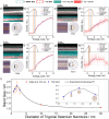
STEM‐EELS Bandgap Analysis of Se NWs Inside BNNTs a) 60 kV HAADF STEM image of Se@BNNT (top), false colour AC‐STEM‐EELS map illustrating semiconducting (pink) and insulating (cyan) regions, respectively, of the area shown above (middle) and a side on and end on molecular model of the Se@BNNT shown above, b) curve fitting of the ultra‐low‐loss EEL spectrum corresponding to the encapsulated Se shown in a), c) and d), e) and f) and g) and h) show the same as a) and b) but for Se NWs of different diameters, i) shows a summary of the bandgap energies of t‐Se NWs as their diameter is reduced, fitted to an exponential growth‐decay curve to guide the eye.

References

    1. Boyd R., Nat. Chem. 2011, 3, 570. - PubMed
    1. Smith W., Nature 1873, 7, 303.
    1. Smith W., J. Soc. Telegraph Eng. 1873, 2, 31.
    1. Adams W. G., Day R. E., Phil. Trans. R. Soc. 1877, 167, 313.
    1. Fritts C. E., Am. J. Sci. 1883, s3‐26, 465.

LinkOut - more resources