Review
. 2025 May 11;15(10):724.
doi: 10.3390/nano15100724.

A Review of Nanowire Devices Applied in Simulating Neuromorphic Computing

Affiliations
Review

A Review of Nanowire Devices Applied in Simulating Neuromorphic Computing

Tianci Huang et al. Nanomaterials (Basel). .

Abstract

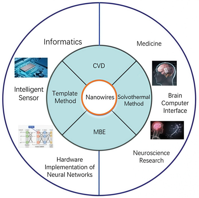
With the rapid advancement of artificial intelligence and machine learning technologies, the demand for enhanced device computing capabilities has significantly increased. Neuromorphic computing, an emerging computational paradigm inspired by the human brain, has garnered growing attention as a promising research frontier. Inspired by the human brain's functionality, this technology mimics the behavior of neurons and synapses to enable efficient, low-power computing. Unlike conventional digital systems, this approach offers a potentially superior alternative. This article delves into the application of nanowire materials (and devices) in neuromorphic computing simulations: First, it introduces the synthesis and preparation methods of nanowire materials. Then, it analyzes in detail the key role of nanowire devices in constructing artificial neural networks, especially their advantages in simulating the functions of neurons and synapses. Compared with traditional silicon-based material devices, it focuses on how nanowire devices can achieve higher connection density and lower energy consumption, thereby enabling new types of neuromorphic computing. Finally, it looks forward to the application potential of nanowire devices in the field of future neuromorphic computing, expecting them to become a key force in promoting the development of intelligent computing, with extensive application prospects in the fields of informatics and medicine.

Keywords: nanowire devices; neural network; neuromorphic computing.


Conflict of interest statement

The authors declare no conflict of interest.

Figures

Figure 15
Figure 15
(a) NW synaptic memristor for pattern recognition using WO3. (b) The process of backpropagation algorithm. (c) Simulation of MNIST pattern recognition based on Si NW synaptic FeFET. (d) Application of LTP/LTD in ZnO NW optoelectronic synaptic transistors. (e) The changes in current weight during the enhancement and inhibition process of ZnO NW synaptic transistors. (f) Recognition accuracy [47]. Copyright 2023, IOP Publishing Ltd. (a) [50] Copyright 2022, AIP Publishing. (b,c) Reprinted from Ref. [58] (d,f) [86] Copyright 2021, IOP Publishing Ltd.
Figure 16
Figure 16
(a) Dependence between recognition rate and training iterations in ionic-gated Si NW synaptic FET SNN. (b) Dependency between recognition rate and output neurons. (c) Core–shell dual-gate NW synaptic transistor for HNN. (d) Recognition accuracy of HNN when image is 28 × 28 pixels. (e) Schematic diagram of single-layer perceptron HNN. (f) Training outcomes. (g) Schematic diagram of Ag NW network resistive memristive device used for reservoir calculation [47]. Copyright 2023, IOP Publishing Ltd. (a,b) [59] Copyright 2020, RSC Pub. (c,d) Reprinted from Ref. [88]. (e,f) [89] Copyright 2021, Elsevier Ltd. (g) Reprinted from Ref. [91].
Figure 1
Figure 1
Synthesis methods and application fields of nanowires.
Figure 2
Figure 2
Preparation of single crystal iron nanowires by CVD [28]. Copyright 2015, Elsevier B.V.
Figure 3
Figure 3
Schematic diagram of the AAO template [31]. Copyright 2019, American Chemical Society.
Figure 4
Figure 4
Schematic diagram of the preparation of copper nanowires by liquid crystal template method [34]. Copyright 2012, American Chemical Society.
Figure 5
Figure 5
(af) Schematic diagram of the growth mechanism of copper nanowires prepared by solvothermal method. Reprinted from Ref. [35].
Figure 6
Figure 6
(a) Scanning electron microscopy (SEM) image showing a set of Au-assisted arrays of GaAs NWs [36]. Copyright 2018, AIP Publishing. (b) High-resolution transmission electron mi-croscopy (HRTEM) image of a single GaAs NW edge [38]. Copyright 2007, IOP Publishing.
Figure 7
Figure 7
(a) An oxide mask (SiOx) is formed on silicon (Si), and a series of holes with a diameter of D (usually 50–100 nm) and a period of P (usually a few hundred nm) are patterned by photolithography. (b) Vapor phase growth of NWs. The MBE growth is described in a condition that includes group III atoms (e.g., Ga) and group V dimers (e.g., As2) in a gas phase flux. Group III droplets (e.g., Ga) are formed in the pores. (c) Nucleation of NWs on Ga droplets located in the wells [36]. Copyright 2018, AIP Publishing.
Figure 8
Figure 8
HAADF-STEM images reveal the GaAs (bright contrast) and GaP (dark contrast) regions in (a) a cross-sectional view of the NW core–shell structure and (b) an axial NW structure, with insets showing magnified views [36]. Copyright 2018, AIP Publishing.
Figure 9
Figure 9
(a) Device structure diagram of Ag NWs coated with TiO2 network. (b) I–V curve [48]. Copyright 2020, Wiley-VCH GmbH.
Figure 10
Figure 10
(a) Structure of TiO2 NW-based memory devices before and after plasma treatment. (b) I-V curve of original TiO2 NWs. (c) I-V curves of TiO2 NWs after Ar-H2 plasma treatment. (d) Excitatory postsynaptic current (EPSC) of devices treated with different gas plasmas. (e) Short-term dependent plasticity (SNDP). (f) STDP. (g) Synaptic schematic diagram and scanning electron microscopy (SEM) image of single ZnO NW memory. (h) I-V curve of device. (i) STDP. (j) Short-term rate-dependent plasticity (SRDP). (k) Short-term rate-dependent plasticity (SVDP). (l) Relationship between conductivity and number of pulses [47]. Copyright 2023, IOP Publishing Ltd. (af) [54] Copyright 2020, Wiley-VCH GmbH. (gl) [52] Copyright 2019, IOP Publishing.
Figure 11
Figure 11
(a) Scheme of Si NW-based synaptic FeFET. (b) Transfer characteristics of Si NW FeFET with different scanning ranges. (c) The dependence of EPSC on pulse voltage. (d) SNDP. (e) LTP/LTD. Reprinted from Ref. [58].
Figure 12
Figure 12
(a) Schematic diagram of the ionic-gated Si NW synaptic FET. (b) The transfer characteristics of the device under two gates modulation. (c) Short-term enhancement and long-term enhancement. (d) Paired pulse facilitation. (e) SRDP. (f) The dependence of linear factor on pulse voltage [59]. Copyright 2023, Tsinghua University Press.
Figure 13
Figure 13
(a) Three-dimensional schematic of single silicon nanowire-based neuronal device. (b) Corresponding cross-sectional view. (c) Output characteristics (I–V curves) of single silicon nanowire neuronal device in gate-drain connected configuration. Reprinted from Ref. [69].
Figure 14
Figure 14
Energy band diagrams and recombination rates of single silicon nanowire neural device during integration, triggering, and reset response periods: (a) leakage integrated states at Vin = 0.50, 0.70, and 1.00 V, during forward scanning; (b) Vin state = 1.15 V; and (c) reset state has Vin values = 0.80, 0.70, and 0.50 V (during reverse scanning). Reprinted from Ref. [69].

Similar articles

References

    1. Wang X., Wang R., Shi L., Sun J. Synthesis of metal/bimetal nanowires and their applications as flexible transparent electrodes. Small. 2015;11:4737–4744. doi: 10.1002/smll.201501314. - DOI - PubMed
    1. Furber S. Large-scale neuromorphic computing systems. J. Neural Eng. 2016;13:051001. doi: 10.1088/1741-2560/13/5/051001. - DOI - PubMed
    1. Schlatterer K. Universität Tübingen; Tübingen, Germany: 2022. Immune modulation by molecules of Staphylococcus aureus.
    1. Hasler J., Marr B. Finding a roadmap to achieve large neuromorphic hardware systems. Front. Neurosci. 2013;7:118. doi: 10.3389/fnins.2013.00118. - DOI - PMC - PubMed
    1. Merces L., Ferro L.M.M., Nawaz A., Sonar P. Advanced Neuromorphic Applications Enabled by Synaptic Ion-Gating Vertical Transistors. J Adv. Sci. 2024;11:2305611. doi: 10.1002/advs.202305611. - DOI - PMC - PubMed

LinkOut - more resources