. 2025 Apr 8;6(5):563-576.
doi: 10.1021/accountsmr.4c00349. eCollection 2025 May 23.

Advancing Thermal Management Technology for Power Semiconductors through Materials and Interface Engineering

Affiliations

Advancing Thermal Management Technology for Power Semiconductors through Materials and Interface Engineering

Man Li et al. Acc Mater Res. .

Abstract

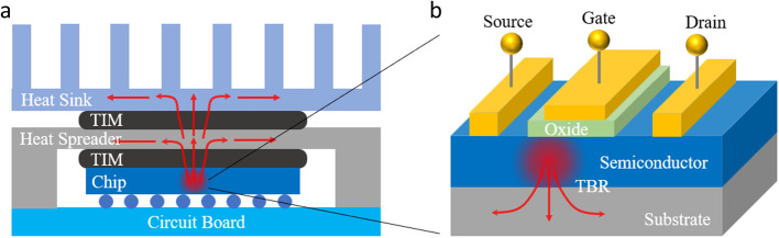
Power semiconductors and chips are essential in modern electronics, driving applications from personal devices and data centers to energy technologies, vehicles, and Internet infrastructure. However, efficient heat dissipation remains a critical challenge, directly affecting their performance, reliability, and lifespan. High-power electronics based on wide- and ultrawide-bandgap semiconductors can exhibit power densities exceeding 10 kW/cm2, hundreds of times higher than digital electronics, posing significant thermal management challenges. Addressing this issue requires advanced materials and interface engineering, alongside a comprehensive understanding of materials physics, chemistry, transport dynamics, and various electronic, thermal, and mechanical properties. Despite progress in thermal management solutions, the complex interplay of phonons, electrons, and their interactions with material lattices, defects, boundaries, and interfaces presents persistent challenges. This Account highlights key advancements in thermal management for power semiconductors and chips, with a focus on our group's recent contributions. Our approach addresses several critical issues: (1) developing materials with ultrahigh thermal conductivity for enhanced heat dissipation, (2) reducing thermal boundary resistance between power semiconductors and emerging 2D materials, (3) improving thermal and mechanical contacts between chips and heat sinks, (4) innovating dynamic thermal management solutions, and (5) exploring novel principles of thermal transport and design for future technologies. Our research philosophy integrates multiscale theoretical predictions with experimental validation to achieve a paradigm shift in thermal management. By leveraging first-principles calculations, the recent studies redefined traditional criteria for high-thermal-conductivity materials. Guided by these insights, we developed boron arsenide and boron phosphide, which exhibit record-high thermal conductivities of up to 1300 W/mK. Through phonon band structure engineering, we reduced TBR in GaN/BAs interfaces by over 8-fold compared to GaN/diamond interfaces. The combination of low TBR and high thermal conductivity significantly reduced hotspot temperatures, setting new benchmarks in thermal design for power electronics. We further explored the anisotropic TBR properties of two-dimensional materials and Moiré patterns in twisted graphene, expanding the thermal design landscape. To address challenges at device-heat sink interfaces, we developed self-assembled boron arsenide composites with a thermal conductivity of 21 W/mK and exceptional mechanical compliance (∼100 kPa). These composites provide promising solutions for thermal management in flexible electronics and soft robotics. In dynamic thermal management, we pioneered the concept of solid-state thermal transistors, enabling electrically controlled heat flow with unparalleled tunability, speed, reliability, and compatibility with integrated circuit fabrication. These innovations not only enhance thermal performance but also enable the exploration of novel transport physics, improving our fundamental understanding of thermal energy transport under extreme conditions. Looking forward, we reflect on remaining challenges and identify opportunities for further advancements. These include scaling up the production of high-performance materials, integrating thermal solutions with existing manufacturing processes, and uncovering new physics to inspire next-generation power electronics technologies. By addressing these challenges, we aim to inspire future codesign strategies that enable the development of more efficient, reliable, sustainable, and high-performance electronic systems.


Figures

1
1
Thermal crisis history of electronics and the technology roadmap for resolving the challenges. The red data points indicate the power density increase from less than 10 W/cm2 for the earliest central processing units to nearly 1 MW/cm2 projected for local hot spots in GaN power electronics, which triggered many government-funded attempts, as exemplified by the US programs (dark blue boxes) and European Union programs (light blue boxes). The inset plot shows the strong dependence of GaN device lifetime on temperature derived by a program performer.
2
2
Thermal management design of electronics, including optimization of (a) heat sinks, heat spreaders, thermal interface materials, and others at the device or package level and (b) the thermal boundary resistance and cooling substrate at the near-junction region of transistors.
3
3
Material synthesis and structural and thermal characterization of the single crystal of boron phosphide (BP). The crystals are characterized with the (a) scanning electron microscope image and (b) powder X-ray diffraction patterns. The scale bar is 50 μm. (c) The experimentally measured temperature-dependent thermal conductivity of BP shows a reduction from ∼1400 to 460 W/mK, captured by the modeling fit considering multiple phonon scattering processes. (d) The extracted intrinsic thermal conductivity of isotope-free BP decreases from 26000 to 1400 W/mK over a temperature range from 77 to 298 K, in comparison with the calculation results from DFT. Reproduced with permission from ref . Copyright 2017 American Chemical Society.
4
4
Experimental investigation of exceptional thermal conductivity and unusual phonon transport characteristics in boron arsenide (BAs). (a) Illustration of the zinc-blende crystal structure for cubic BAs. (b) High-resolution transmission electron microscope image displaying the BAs lattice structure and dimensions, with an inset diffraction pattern along the [111] zone axes. Scale bar: 2 nm. (c) Temperature-dependent thermal conductivity of BAs in the range of 300–600 K, benchmarked against diamond and cubic BN. (d) Phonon mean free path spectra for BAs from heater size-dependent thermal experiments, in comparison with theory. Reproduced with permission from ref . Copyright 2018 American Association for the Advancement of Science.
5
5
Exploration of high-thermal-conductivity materials among ternary and two-dimensional materials. (a) Temperature-dependent thermal conductivity of three different phases of BNC2, BPC2, and BAsC2 in comparison to diamond, BAs, BN, and BP. (b) Thermal conductivity prediction of two-dimensional BN, BP, BAs, and BSb in comparison with graphene, silicene, and germanene. Reproduced with permission from refs and . Copyright 2021 and 2019 American Physical Society.
6
6
Interface thermal transport and thermal boundary resistance (TBR). (a) TBR, ascertained from the temperature discontinuity at the interface, can result from phonon scattering at the interface, incomplete contact, and interface disorder. (b) Debye temperatures of typical high-thermal-conductivity materials and materials commonly utilized in the semiconductor industry. Reproduced with permission from refs and . Copyright 2020 and 2021 Royal Society of Chemistry and The Authors, under exclusive license to Springer Nature Limited.
7
7
Thermal boundary resistance at interfaces between metals and BAs/BP. (a) Ab initio-derived phonon band structures for BAs, BP, diamond, Al, Au, and Pt. (b, c) Experimentally measured temperature-dependent TBR between metals and (b) BAs and (c) BP. Reproduced with permission from ref . Copyright 2021 The Authors, under exclusive license to Springer Nature Limited.
8
8
Integration of BAs and GaN for advanced thermal management. (a) Cross-sectional SEM (left) and high-resolution TEM (right) images showcasing the atomic interface between GaN and BAs layers. (b) Simulated hot-spot temperatures for BAs and diamond as a function of heating size, highlighting the transition from diffusive to ballistic thermal transport using a comparison between Fourier’s heat conduction law and the spectral-dependent Boltzmann transport equation. (c) SEM image of an AlGaN/GaN high-electron-mobility transistor with two fingers, 100 μm width, and 34 μm gate pitch. Scale bar: 20 μm. (d) Experimental measurements of hot-spot temperature increase in operating devices as a function of transistor power density compared to reference GaN-on-diamond and GaN-on-SiC wafers. Reproduced with permission from ref . Copyright 2021 The Authors, under exclusive license to Springer Nature Limited.
9
9
Anisotropic thermal boundary resistance (TBR) across a two-dimensional black phosphorus interface. (a and b) Schematic of interfaces between Al and black phosphorus with zigzag and armchair orientations, respectively. (c) TEM image of the interface between Al and black phosphorus. (d) First-principles-derived phonon dispersion relations along various reciprocal space directions. (e and f) TDTR measurements of temperature-dependent TBR along different directions, in comparison with modeling results. Reproduced with permission from ref . Copyright 2019 Wiley-VCH.
10
10
Flexible thermal interface material with high thermal conductivity based on self-assembled BAs. (a) Schematic to illustrate the self-assembly process, where freeze-drying of BAs suspensions leads to the formation of aligned BAs pillars. (b) Cross-section SEM image of the BAs composite confirms the presence of an aligned lamellar structure. (c) Thermal conductivity of BAs composites with different filler loadings in comparison with the modeling results. (d) Time-dependent infrared images of the LED integrated with different materials (thermal epoxy, silicone thermal pad, and BAs composite) display temperature distributions near the hot spot, highlighting the superior cooling capability of BAs composite compared to conventional materials. Reproduced with permission from ref . Copyright 2021 The Authors.
11
11
Dynamical thermal management using low-dimensional materials. (a) Schematic illustrating dynamic thermal management with precise heat control across spatial and temporal dimensions. (b) Galvanostatic discharge curve for the Li-black phosphorus device. (c) In situ thermal measurement of cross-plane thermal conductivity of electrochemically intercalated black phosphorus. (d) The thermal conductance switching behavior as a function of the gate voltage (V g).. Inset: SEM image of an electrically gated molecular thermal switch. (e) Thermal conductance switching cycles versus scanning frequency up to 1 MHz, measured at every decade. Reproduced with permission from refs and . Copyright 2017 American Chemical Society and 2023 The Authors, some rights reserved; exclusive licensee American Association for the Advancement of Science.
12
12
High-order phonon anharmonicity and non-perturbative interactions in BAs and BP. (a) Schematic of in situ spectroscopy measurements at high pressure with a diamond anvil cell. (b) Pressure-dependent thermal conductivity of BAs at various temperature and pressure. (c) Experimentally measured phonon dispersion from inelastic X-ray scattering (circles), Raman spectroscopy (triangles), and ab initio calculations (lines) under three pressures indicates the interplay of three-phonon and four-phonon scatterings. (d) Phonon dispersion (optical branches) for isotopically pure and naturally abundant BAs. The schematic in the right column illustrates the Brillouin zone folding caused by local and coupled isotope effects. (e) Comparison between calculated (black curve) and experimental (circle) of Raman spectra of BAs with different B isotope concentrations. Reproduced with permission from refs and . Copyright 2022 and 2023 The Authors, under exclusive license to Springer Nature Limited and American Physical Society.

Similar articles

References

    1. Cui Y., Li M., Hu Y.. Emerging Interface Materials for Electronics Thermal Management: Experiments, Modeling, and New Opportunities. J. Mater. Chem. C. 2020;8:10568. doi: 10.1039/C9TC05415D. - DOI
    1. Ravi, S. International technology roadmap for semiconductors (ITRS), 2015. ed.; Semiconductor Industry Association, 2015. https://www.semiconductors.org/resources/2015-international-technology-r....
    1. Li M., Wu H., Avery E. M., Qin Z., Goronzy D. P., Nguyen H. D., Liu T., Weiss P. S., Hu Y.. Electrically Gated Molecular Thermal Switch. Science. 2023;382:585–589. doi: 10.1126/science.abo4297. - DOI - PMC - PubMed
    1. Li S., Qin Z., Wu H., Li M., Kunz M., Alatas A., Kavner A., Hu Y.. Anomalous Thermal Transport under High Pressure in Boron Arsenide. Nature. 2022;612:459–464. doi: 10.1038/s41586-022-05381-x. - DOI - PubMed
    1. Kang J. S., Li M., Wu H., Nguyen H., Aoki T., Hu Y.. Integration of Boron Arsenide Cooling Substrates into Gallium Nitride Devices. Nat. Electron. 2021;4:416–423. doi: 10.1038/s41928-021-00595-9. - DOI

LinkOut - more resources