

Selective metal passivation by vapor-dosed phosphonic acid inhibitors for area-selective atomic layer deposition of SiO2 thin films
- PMID: 40445398
- PMCID: PMC12125412
- DOI: 10.1186/s40580-025-00490-5
Selective metal passivation by vapor-dosed phosphonic acid inhibitors for area-selective atomic layer deposition of SiO2 thin films
Abstract
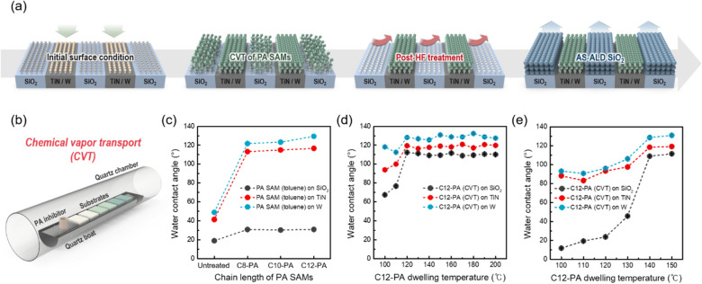
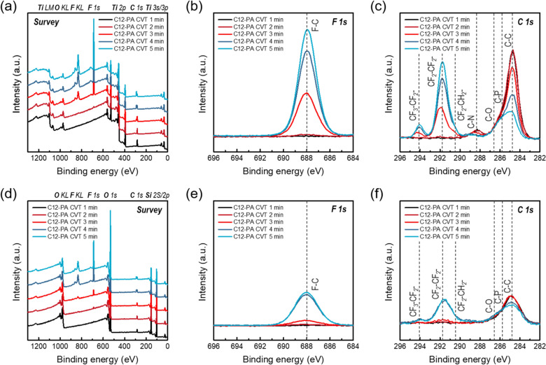
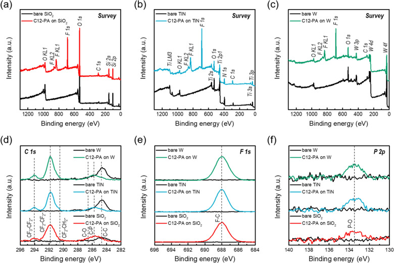
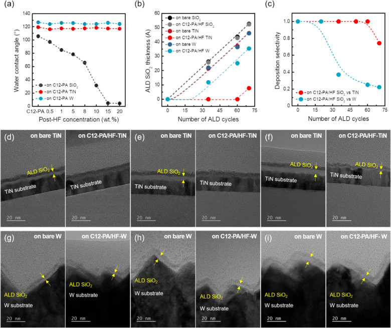
Aiming for atomic-scale precision alignment for advanced semiconductor devices, area-selective atomic layer deposition (AS-ALD) has garnered substantial attention because of its bottom-up nature that allows precise control of material deposition exclusively on desired areas. In this study, we develop a surface treatment to hinder the adsorption of Si precursor on metal surfaces by using a vapor-phase functionalization of bulky phosphonic acid (PA) self-assembled monolayers (SAMs). Through the chemical vapor transport (CVT) method, the bulky solid PA inhibitor with a fluorocarbon terminal group was effectively vaporized, and the conditions for maximizing the blocking effect of the inhibitor were confirmed by optimizing the process temperature and dwelling time. The unintended PA inhibitors adsorbed on SiO2 surfaces during the CVT process were selectively removed by post-HF treatment, thereby leading to selective deposition of SiO2 thin films only on SiO2 substrates. As a results, SiO2 film growth on the PA SAM/HF-treated TiN surfaces was suppressed by up to 4 nm with just a single exposure to the long-chain inhibitor, even during the ALD process using highly reactive O3 reactants. The proposed approach paves the way for highly selective deposition of dielectrics on dielectrics (DoD).
Keywords: Area-selective atomic layer deposition; Chemical vapor transport; Phosphonic acid; Selective removal; Silicon oxide.
© 2025. The Author(s).
Conflict of interest statement
Declarations. Competing interests: The authors declare that they have no competing interests.
Figures


References
-
- G.N. Parsons, R.D. Clark, Area-selective deposition: fundamentals, applications, and future outlook. Chem. Mater. 32(12), 4920–4953 (2020). 10.1021/acs.chemmater.0c00722
-
- J. Zhang, Y. Li, K. Cao, R. Chen, Advances in atomic layer deposition. Nanomanufacturing Metrol. 5(3), 191–208 (2022). 10.1007/s41871-022-00136-8
-
- R. Chen, E. Gu, K. Cao, J. Zhang, Area selective deposition for bottom-up atomic-scale manufacturing. Int. J. Mach. Tools Manuf 199, 104173 (2024). 10.1016/j.ijmachtools.2024.104173
-
- A.J.M. Mackus, A.A. Bol, W.M.M. Kessels, The use of atomic layer deposition in advanced nanopatterning. Nanoscale 6(19), 10941–10960 (2014). 10.1039/C4NR01954G - PubMed
-
- M. Fang, J.C. Ho, Area-selective atomic layer deposition: conformal coating, subnanometer thickness control, and smart positioning. ACS Nano 9(9), 8651–8654 (2015). 10.1021/acsnano.5b05249 - PubMed
Grants and funding
LinkOut - more resources
Full Text Sources
Research Materials
Miscellaneous