. 2025 Jan 7;14(11):1721-1728.
doi: 10.1515/nanoph-2024-0583. eCollection 2025 Jun.

Localized exciton emission from monolayer WS2 nanoribbon at cryogenic temperature

Affiliations

Localized exciton emission from monolayer WS2 nanoribbon at cryogenic temperature

Gang Qiang et al. Nanophotonics. .

Abstract

We conducted low-temperature photoluminescence (PL) spectroscopy experiments on individual WS2 and MoSe2 nanoribbons prepared by gold-assisted exfoliation from the slanted surface of bulk crystals with a vicinal and stepwise pattern. The nanoribbons are predominantly monolayer and have widths varying from hundreds of nanometers down to tens of nanometers. Most MoSe2 NRs display an emission profile similar to 2D excitons of MoSe2 monolayers. In contrast, WS2 nanoribbons are characterized with sharp emission peaks that can be attributed to the emission from localized excitons or trions. Moreover a broad low energy emission peak can be also observed from some of the WS2 nanoribbons, which originates from bilayer regions. In this manuscript, we analyze spectral diffusion behavior along with pump power and temperature dependence of the localized exciton emission peaks, shedding light on potential of TMDC nanoribbons in sensing and opto-electronic applications.

Keywords: WS2 nanoribbon; localized exciton emission; low-temperature photoluminescence.


Conflict of interest statement

Conflict of interest: Authors state no conflicts of interest.

Figures

Figure 1:
Figure 1:
Optical properties of WS 2  and MoSe 2  nanoribbons at low temperature. (a) Optical image of WS2 NRs, the violet background corresponds to the Si/SiO2 substrate, the blue strips are the nanoribbons. (b) Wide-field photoluminescence (PL) image of WS2 NRs, two are covered within the laser spot and marked as L and R, respectively. (c) PL signal of L ribbon dispersed on CCD chip, and (d1)–(d3) corresponding PL spectra from specific pixel positions, namely i – iii in (c) as indicated by the white dashed lines. (e) Wide-field PL image of MoSe2 NRs, three NRs are resolved which are labeled as L, M and R. (f) PL signal of R ribbon dispersed on CCD chip, and (g1) and (g2) corresponding PL spectra from pixel position i – ii in (f) as guided by the white dashed lines. Experiments are done at T = 4.4 K.
Figure 2:
Figure 2:
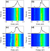
Statistics for sharp emission lines. (a)–(d) PL spectra measured on different WS2 NRs. Statistics of sharp emission line (e) energy and (f) full-width at half maximum (FWHM). The dashed vertical red line marks the exciton (X) emission energy of monolayer WS2. All data are collected at T = 4.4 K.
Figure 3:
Figure 3:
Time-dependent changes of sharp emission lines for four different locations on different nanoribbons. (Upper) PL spectra, (lower) corresponding time traces. Measurements taken at T = 4.4 K.
Figure 4:
Figure 4:
Laser excitation power dependent PL measured on a selected WS2 NR. (a) PL spectra measured under different excitation power. The dotted red lines are fits to five Gaussian peaks (example shown in the top panel). Dashed vertical black lines are guides for eye. (b1) – (b3) Excitation power dependence of the peak position, full-width at half maximum (FWHM), integrated PL intensity for sharp emission peaks, P1 and P2. Experiments are done at T = 4.4 K.
Figure 5:
Figure 5:
Temperature dependent PL emission. (a) PL spectrum of the same WS2 nanoribbon as in Figure 4, measured at various temperatures. (b) PL spectrum at T = 15 K along with the fit using multiple Gaussian functions. Temperature dependence of the peak position, full-width at half maximum (FWHM), integrated PL intensity for (c1)–(c3) sharp emission peaks, P1 and P2.

References

    1. Wang G., et al. Colloquium: excitons in atomically thin transition metal dichalcogenides. Rev. Mod. Phys. . 2018;90(2):021001. doi: 10.1103/revmodphys.90.021001. - DOI
    1. Wilson N. P., Yao W., Shan J., Xu X. Excitons and emergent quantum phenomena in stacked 2D semiconductors. Nature . 2021;599(7885):383–392. doi: 10.1038/s41586-021-03979-1. - DOI - PubMed
    1. Xu X., Yao W., Xiao D., Heinz T. F. Spin and pseudospins in layered transition metal dichalcogenides. Nat. Phys. . 2014;10(5):343–350. doi: 10.1038/nphys2942. - DOI
    1. Yu H., Cui X., Xu X., Yao W. Valley excitons in two-dimensional semiconductors. Natl. Sci. Rev. . 2015;2(1):57–70. doi: 10.1093/nsr/nwu078. - DOI
    1. Atatüre M., Englund D., Vamivakas N., Lee S., Wrachtrup J. Material platforms for spin based photonic quantum technologies. Nat. Rev. Mater. . 2018;3(5):38–51. doi: 10.1038/s41578-018-0008-9. - DOI

LinkOut - more resources