

Deposition of HfO2 by Remote Plasma ALD for High-Aspect-Ratio Trench Capacitors in DRAM
- PMID: 40497832
- PMCID: PMC12156898
- DOI: 10.3390/nano15110783
Deposition of HfO2 by Remote Plasma ALD for High-Aspect-Ratio Trench Capacitors in DRAM
Abstract
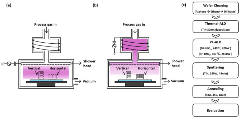
Dynamic random-access memory (DRAM) is a vital component in modern computing systems. Enhancing memory performance requires maximizing capacitor capacitance within DRAM cells, which is achieved using high-k dielectric materials deposited as thin, uniform films via atomic layer deposition (ALD). Precise film deposition that minimizes electronic defects caused by charged vacancies is essential for reducing leakage current and ensuring high dielectric strength. In this study, we fabricated metal-insulator-metal (MIM) capacitors in high-aspect-ratio trench structures using remote plasma ALD (RP-ALD) and direct plasma ALD (DP-ALD). The trenches, etched into silicon, featured a 7:1 aspect ratio, 76 nm pitch, and 38 nm critical dimension. We evaluated the electrical characteristics of HfO2-based capacitors with TiN top and bottom electrodes, focusing on leakage current density and equivalent oxide thickness. Capacitance-voltage analysis and X-ray photoelectron spectroscopy (XPS) revealed that RP-ALD effectively suppressed plasma-induced damage, reducing defect density and leakage current. While DP-ALD offered excellent film properties, it suffered from degraded lateral uniformity due to direct plasma exposure. Given its superior lateral uniformity, lower leakage, and defect suppression, RP-ALD shows strong potential for improving DRAM capacitor performance and serves as a promising alternative to the currently adopted thermal ALD process.
Keywords: atomic layer deposition; capacitor; leakage current; plasma damage; remote plasma ALD; step coverage; thermal ALD; trench structure.
Conflict of interest statement
The authors declare no conflicts of interest. The funder had no role in the design of the study; in the collection, analyses, or interpretation of the data; in the writing of the manuscript; or in the decision to publish the results.
Figures


References
-
- Smitha P.S., Babu V.S., Shiny G. Critical parameters of high performance metal-insulator-metal nanocapacitors: A Review. Mater. Res. Express. 2019;6:122003. doi: 10.1088/2053-1591/ab5511. - DOI
-
- An C.H., Lee W., Kim S.H., Cho C.J., Kim D.-G., Kwon D.S., Cho S.T., Cha S.H., Lim J.I., Jeon W., et al. Controlling the electrical characteristics of ZrO2/Al2O3/ZrO2 capacitors by adopting a Ru top electrode grown via atomic layer deposition. Phys. Status Solidi (RRL)–Rapid Res. Lett. 2019;13:1800454. doi: 10.1002/pssr.201800454. - DOI
-
- Zheng G., He Y.-L., Zhu B., Wu X., Zhang D.W., Ding S.-J. Improvement of voltage linearity and leakage current of MIM capacitors with atomic layer deposited Ti-doped ZrO2 insulators. IEEE Trans. Electron. Devices. 2023;70:3064–3070. doi: 10.1109/TED.2023.3267752. - DOI
-
- Cho H.J., Kim Y.D., Park D.S., Lee E., Park C.H., Jang J.S., Lee K.B., Kim H.W., Chae S.J., Ki Y.J., et al. New TIT capacitor with ZrO2/Al2O3/ZrO2 dielectrics for 60 nm and below DRAMs; Proceedings of the 2006 European Solid-State Device Research Conference; Montreux, Switzerland. 19–21 September 2006; pp. 146–149.
LinkOut - more resources
Full Text Sources
