Review
. 2025 Jun 9;18(12):2714.
doi: 10.3390/ma18122714.

Overview on the Thermally Activated Delayed Fluorescence and Mechanochromic Materials: Bridging Efficiency and Versatility in LECs and OLEDs

Affiliations
Review

Overview on the Thermally Activated Delayed Fluorescence and Mechanochromic Materials: Bridging Efficiency and Versatility in LECs and OLEDs

Raheleh Ghahary et al. Materials (Basel). .

Abstract

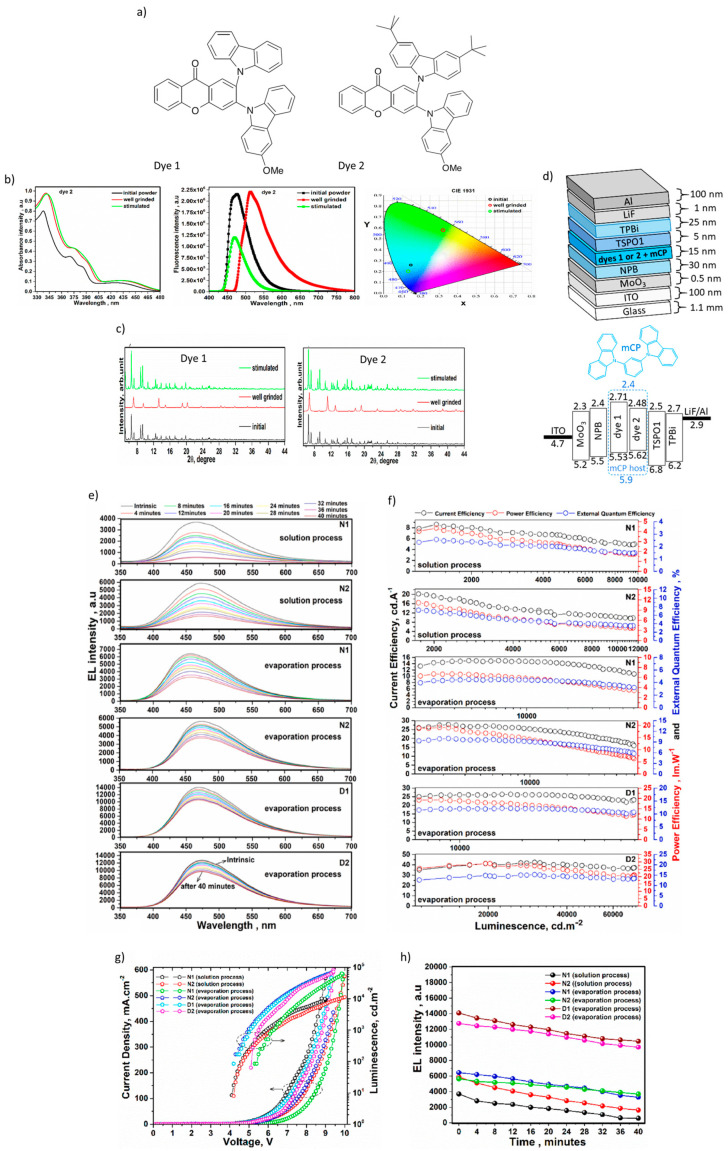
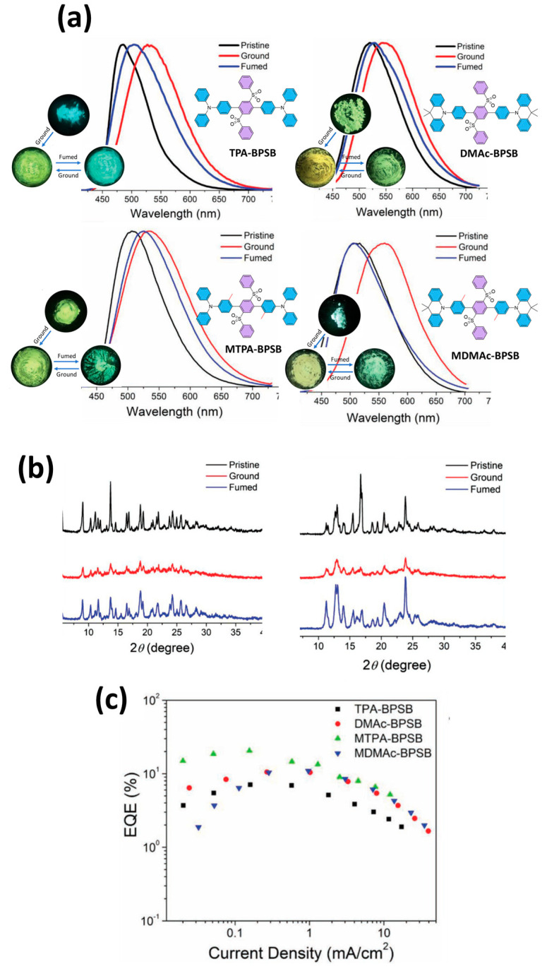
Recent advancements in thermally activated delayed fluorescence (TADF) materials and mechanochromic materials have significantly enhanced the efficiency and versatility of light-emitting electrochemical cells (LECs) and organic light-emitting diodes (OLEDs). TADF materials have enabled efficiency improvements, achieving an internal quantum efficiency (IQE) of nearly 100% by utilizing both singlet and triplet excitons. Meanwhile, mechanochromic materials exhibit reversible optical changes upon mechanical stimuli, making them promising for stress sensing, encryption, and flexible electronics. The synergistic integration of TADF and mechanochromic materials in OLEDs and LECs has led to enhanced efficiency, stability, and multifunctionality in next-generation lighting and display technologies. This narrative review explores recent breakthroughs in devices that incorporate both TADF and mechanochromic materials as emitters. Particular attention is given to the molecular design that enable both TADF and mechanochromic properties, as well as optimal device structures and performance parameters. Moreover, this review discusses the only LEC fabricated so far using a TADF-mechanochromic emitter, highlighting its performance and potential. Finally, the report concludes with an outlook on the future commercial applications of these materials, particularly in wearable electronics and smart display technologies.

Keywords: light-emitting electrochemical cells (LECs); mechanochromic; organic light-emitting diodes (OLEDs); reverse intersystem crossing (RISC); thermally activated delayed fluorescence (TADF).


Conflict of interest statement

The authors declare no conflict of interest.

Figures

Figure 3
Figure 3
Schematic representations of LEC configurations and materials: (a) sandwich configuration, (b) surface configuration with interdigitated electrodes, and (c) chemical structures of various emitters and ionic additives adapted and redrawn from [19,23].
Figure 1
Figure 1
An overview of mentioned TADF and mechanochromic properties characterization methods.
Figure 2
Figure 2
An overview of mentioned devices (OLEDs and LECs) characterization methods.
Figure 4
Figure 4
Energy-level diagrams illustrating operation of LECs: (a) transient response at eV < Eg, (b) transient response at eV = Eg, and (c) steady-state operation at eV > Eg. Larger circles depict ions, small open circles represent holes, and small solid circles represent electrons, Adapted and redrawn from [20].
Figure 5
Figure 5
Structure of (a) an OLED and (b) a LEC, adapted and redrawn from [23].
Figure 6
Figure 6
Radiative deactivation pathways existing in (a) fluorescent, (b) phosphorescent, (c) TADF, and (d) TTA [76].
Figure 7
Figure 7
Strategy of realizing small ΔEST in organic molecules, adapted and redrawn from [77].
Figure 8
Figure 8
(a) Temperature dependence of transient PL-decay spectra, (b) temperature dependence of transient PL spectrum, (c) power dependence of delayed fluorescence, and (d) straight linear fit of delayed fluorescence intensity as a function of excitation power of spin-coated (DMAC-TRZ)-doped compound on solid film [76].
Figure 9
Figure 9
(a) Molecular structures of dye 1 and dye 2. (b) Absorption and emission spectra, and CIE chromaticity diagram of dye 2 under the well grinded and stimulated modes. (c) XRD patterns of dye 1, and dye 2 at initial, well grinded, and stimulated modes. (d) Structure of OLEDs and energy level diagram of employing doped (evaporation process). (e) Stability of electroluminescence spectra. (f) Current–power and external quantum efficiency versus luminance plots of non-doped and doped OLEDs. (g) Current density voltage–luminance plots of non-doped and doped OLEDs. (h) Variations of electroluminescence intensity over utilization time [96].
Figure 10
Figure 10
(a) Molecular structures of target compounds, Photographs and PL spectra of (b) 5TzPmPXZ, (c) 7TzPmPXZ, and (d) 5,7TzPmPXZ in response to external stimuli. Photographs were taken under UV irradiation with 365 nm. (grinding with a mortar and a pestle; heating at 150 °C for 5TzPmPXZ and 7TzPmPXZ, 200 °C for 5,7TzPmPXZ; fuming with CH2Cl2 vapor; recrystallization from n-hexane/CHCl3), PXRD patterns of (e) 5TzPmPXZ, (f) 7TzPmPXZ, and (g) 5,7TzPmPXZ, (h) Luminance–voltage–current density curves for devices A, B, and C (inset: the normalized EL spectra of devices). (i) External quantum efficiency and current efficiency versus luminance curves for devices A, B, and C (inset: The energy level diagrams for the devices A, B, and C). Reanalyzed and modified from data reported in [102].
Figure 11
Figure 11
(a) Molecular structures of TATC-BP and TATP-BP, and Fluorescent images (under UV illumination) of the pristine crystalline, ground, and vapor fumed powders of TATC-BP and TATP-BP. Normalized PL spectra of TATC-BP (b) and TATP-BP (c) (excitation wavelength: 365 nm), Powder X-ray diffraction patterns of TATC-BP (d) and TATP-BP (e) before and after grinding, and after fuming treatment of the ground solid with dichloromethane, (f) Current density–voltage–luminance and, (g) external quantum efficiency–luminance characteristics. Inset: EL spectra of the OLED devices at 1000 cd m−2, (h) Current efficiency/luminance/power efficiency curves of the nondoped devices of TATC-BP and TATP-BP, Inset: device configuration. Reanalyzed and modified from data reported in [105].
Figure 12
Figure 12
(a) Photographs and PL spectra of QBP-DMAC in response to external stimuli. Photographs were taken under UV irradiation at 365 nm. (grinding with a mortar and a pestle; fuming with CH2Cl2 vapor; recrystallization from n-hexane/CH2Cl2). (b) PXRD patterns of QBP-DMAC, (c) EQE versus luminance curves of the devices. Inset: Normalized EL spectra and device structure. (d) Luminance–voltage–current density curves of the devices. Reanalyzed and modified from data reported in [106].
Figure 13
Figure 13
(a) Photoluminescence spectra of T2 in single crystal (black), powder (red), sublimation state (blue) and ground state (green) respectively, (b) Photo-graphic images of the color and luminescence changes of T2 in response to mechanical grinding: (A) and (C) unground sample, (B) and (D) ground sample. Photographs were taken under ambient light and UV irradiation (365 nm), (c) Current density-voltage-luminance, (d) EL spectra of the blue OLEDs, (e) external quantum efficiency-luminance plots. Reanalyzed and modified from data reported in [107].
Figure 14
Figure 14
(a) Molecular structures of organic emitters. (b) Photographs of mechanochromic emission in response to external stimuli. (c) Energy band diagram of non-doped OLEDs. (d) Normalized electroluminescence spectra. (e) CIE 1931 coordinates. (f) Current efficiency, (g) power efficiency, and (h) external quantum efficiency of triplet-harvesting non-doped OLEDs [108].
Figure 15
Figure 15
(a) Molecular structure of the emitters. (b) Photographs of DCNQ-DMAC taken under a 365 nm UV lamp after crushing or exposure to dichloromethane vapors. (c) Normalized fluorescence spectra of DCNQ-DMAC in different states of aggregation. (d) XRD curves of DCNQ-DMAC in different states of aggregation. (e) Doped device structure and energy level diagram of the materials. (f) Current density–voltage–luminance curves for the three compounds. (g) Current efficiency, power efficiency, and EQE as a function of luminance for the three compounds. (h) Normalized electroluminescence (EL) spectrum [109].
Figure 16
Figure 16
(a) Steady-state (PL) photoluminescence spectra of 2BPy-mTC. (b) Powder X-ray diffraction pattern (PXRD) of 2BPy-mTC. (c) Photographs showing MCL color changes observed under UV irradiation (365 nm) in response to external stimuli. (d) Architecture of device and energy level diagram. (e) Molecular structure of 2BPy-mTC. (f) Current density–voltage–luminance (J-V-L) curves. (g) EQE/luminance curves (EQE-L) of devices with normalized EL spectra [110].
Figure 17
Figure 17
(a) Molecular structures of DMAC-3FDPS and DMAC-2FDPS, and photographs of the two isomers in response to external stimuli, taken in daylight and UV irradiation (365 nm). (b) Photoluminescence spectra (PL) of the two isomers in response to external stimuli, taken in daylight and UV irradiation (365 nm). (c) XRD patterns of the two isomers in different states, (d) EQE, CE and PE luminance curves, Inset: Electroluminescence (EL) spectra of the non-doped OLEDs. Reanalyzed and modified from data reported in [111].
Figure 18
Figure 18
(a) Molecular structure of mDCBP, and photos of mDCBP in its different states: (a) crystalline, (b) after grinding, (c) after solvent diffusion, (d) writing of “NTHU”, (e) erasure of letters by solvent diffusion and (f) writing of “TADF” on the material. (b) Emission spectra of mDCBP in crystalline, amorphous and glassy form (insets: corresponding photos under UV light). (c) Powder X-ray diffraction (PXRD) patterns of mDCBP. (d) Current efficiency versus luminance of devices A–D (inset: EQE of devices A–D). Reanalyzed and modified from data reported in [112].
Figure 19
Figure 19
(a) Molecular structure of target emitters. (b) Photoluminescence (PL) spectra (λexc = 450 nm) of prepared, sublimated, and polished samples of tBuTPA-BQ, as well as corresponding photos under UV light (λexc = 365 nm). (c) PXRD patterns of prepared, sublimed, and ground samples of tBuTPA-BQ. (d) PL spectra (λexc = 450 nm) of prepared, ground, and EtOAc-coated samples of TPPA-BQ, as well as corresponding photos under UV light (λexc = 365 nm). (e) PXRD pattern of TPPA-BQ samples in initial state, milled, and smoked in EtOAc. (f) Repeated change of photoluminescence emission wavelength with mechanical pressure and EtOAc treatment. (g) Demonstration of writing and erasing on filter paper, with photographs taken under daylight and UV light (λexc = 365 nm). (h) Energy level diagram of materials used in devices. (i) Current density and luminance as a function of voltage for devices. (j) EQE curves as a function of luminance for devices. (k) Electroluminescence spectra (EL) of devices (inset: photos of the EL of devices) [113].
Figure 20
Figure 20
(a) Molecular structures of the compounds, and PL spectra and photographs of TPA-BPSB, DMAc-BPSB, MTPA-BPSB and MDMAc-BPSB under different external stimuli, and the photographs were taken under UV ir-radiation at λexc = 365 nm. (b) PXRD patterns of MTPA-BPSB and MDMAc-BPSB at room temperature under different external stimuli. (c) EQE current density curves of the devices. Reanalyzed and modified from data reported in [114].
Figure 21
Figure 21
(a) Molecular structures of XT-DPDBA and XT-BDPDBA. (b) Photoluminescence (PL) spectra of untreated crystals and ground samples. (c) PL spectra of ground samples of XT-DPDBA in response to external stimuli (H: heating at 200 °C for 1 h, F: fuming with CH₂Cl₂ for 1 h, G: grinding with a mortar for 30 min). (d) PL spectra of milled samples of XT-BDPDBA under same excitation conditions. (e) Repeated mechanochromic behavior of XT-DPDBA: grinding and heating (top) and grinding and smoking (bottom), with corresponding photographs of samples under 365 nm UV irradiation. (f) Photographs of samples after grinding, heating, and smoking. (g) PXRD patterns of crystals and milled samples of XT-DPDBA. (h) PXRD patterns of crystals and ground samples of XT-BDPDBA. (i) Electroluminescence (EL) spectra of XT-BDPDBA at 10 mA-cm−2. (j) Luminance–voltage–current density (L–V–J) curves of XT-BDPDBA. (k) EQE and luminance curves of XT-BDPDBA [115].
Figure 22
Figure 22
(a) Photos of five aggregates of 4CzPTANMe under UV excitation (λexc = 365 nm). (b) Molecular structure of 4CzPTANMe. (c) Fluorescence image of C5 in a dish (left: as prepared, right: ground with DCM). (d) Fluorescence spectra (FL) of 4CzPTANMe in different solid states. (e) XRD spectra of 4CzPTANMe in different solid states. (f) Luminance–voltage–current density (L–V–J) curves. (g) Curves of current efficiency and power efficiency as a function of luminance. (h) Normalized electroluminescence (EL) spectra. (i) Schematic energy level diagrams of devices [116].
Figure 23
Figure 23
(a) Fluorescence photos and PL spectra of crystal Y and crystal-R in response to external stimuli. The photos were taken under UV irradiation (λexc = 365 nm). (b) PXRD patterns of crystal-Y, milled samples and heated samples, and crystal-R, milled samples and smoked samples, (c) Electroluminescence spectra (EL) recorded at 100 cd.m−2. Inset: (Current density–voltage–brightness (J–V–L) curves). (d) Molecular structure of TPA-DQP and Schematic representation of the OLED device architecture, (e) PE and CE as a function of luminance of TPA-DQP-based devices. (f) EQE curves as a function of current density. Reanalyzed and modified from data reported in [117].
Figure 24
Figure 24
(a) Powder X-ray diffraction (XRD) patterns of before and after stimulation of dyes 1 and 2, and (b) PL spectrum of before and after stimulation of dyes 1 and 2. (c) (A) Applied voltage vs. brightness and current density, (BD) current, power, and external quantum efficiency curves. (d) Molecular structure of dye 1 and dye 2. (e) Energy level of LEC structure [118].

Similar articles

References

    1. Nakanotani H., Tsuchiya Y., Adachi C. Thermally-activated Delayed Fluorescence for Light-emitting Devices. Chem. Lett. 2021;50:938–948. doi: 10.1246/cl.200915. - DOI
    1. Dias F.B., Bourdakos K.N., Jankus V., Moss K.C., Kamtekar K.T., Bhalla V., Santos J., Bryce M.R., Monkman A.P. Triplet Harvesting with 100% Efficiency by Way of Thermally Activated Delayed Fluorescence in Charge Transfer OLED Emitters. Adv. Mater. 2013;25:3707–3714. doi: 10.1002/adma.201300753. - DOI - PubMed
    1. Zhao K., Zhao Y., Qian R., Ye C., Song Y. Recent Advances in Interactive Mechanosensory Electronics with Luminescence/Coloration Outputs for Wearable Applications. ACS Mater. Lett. 2023;5:3093–3116. doi: 10.1021/acsmaterialslett.3c00800. - DOI
    1. Weder C. Encyclopedia of Polymeric Nanomaterials. Springer; Berlin/Heidelberg, Germany: 2013. Mechanochromic Polymers; pp. 1–11. - DOI
    1. Dos Santos J.M., Hall D., Basumatary B., Bryden M., Chen D., Choudhary P., Comerford T., Crovini E., Danos A., De J., et al. The Golden Age of Thermally Activated Delayed Fluorescence Materials: Design and Exploitation. Chem. Rev. 2024;124:13736–14110. doi: 10.1021/acs.chemrev.3c00755. - DOI - PMC - PubMed

LinkOut - more resources