

Impact of Argon, Nitrogen, and Oxygen Exposure on the Structural and Optoelectrical Properties of Mixed Tin-Lead Halide Perovskites
- PMID: 40584377
- PMCID: PMC12198983
- DOI: 10.1021/acsomega.5c00956
Impact of Argon, Nitrogen, and Oxygen Exposure on the Structural and Optoelectrical Properties of Mixed Tin-Lead Halide Perovskites
Abstract
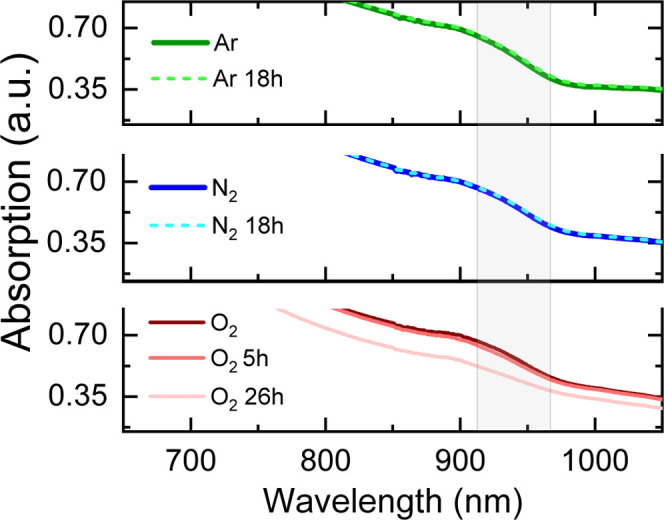
Mixed tin-lead halide perovskites are considered promising materials for narrow-bandgap photovoltaic applications, particularly in tandem solar cells. However, their practical implementation is hindered by stability issues, especially due to tin oxidation and trap-state formation. In this study, we investigate the impact of argon, nitrogen, and oxygen storage environments on the structural, optical, and electronic properties of mixed tin-lead halide CsFAPb0.5Sn0.5I3 perovskites. Optical absorption, transient photoluminescence (PL), transient photocurrent, and time-delayed collection field (TDCF) measurements reveal the significant role of environmental conditions on carrier dynamics. Carrier trapping over tens of nanoseconds is observed in samples prepared and stored in argon, with a trapping rate increasing several times after exposure to nitrogen (with less than 0.1 ppm of oxygen) and further increasing upon exposure to O2. Photocurrent transients also show a fast photocurrent decay component occurring within tens of nanoseconds, independent of the oxygen-created traps. Based on the TDCF measurements, we attribute this fast photocurrent decay component to the spatial traps created by the perovskite boundaries, which reduce the carrier mobility to values below 0.05 cm2/V·s, as estimated from transient photocurrent measurements. Our findings highlight the importance of carefully controlling fabrication and storage conditions, often overlooked due to their initially minor impact on device performance, as these conditions critically affect material stability and charge carrier dynamics.
© 2025 The Authors. Published by American Chemical Society.
Figures


Similar articles
-
Impact of Solvent-Induced Surface Restructuring on Charge Carrier Dynamics in DMASnI3.ACS Appl Mater Interfaces. 2025 Jun 18;17(24):35552-35561. doi: 10.1021/acsami.5c05852. Epub 2025 Jun 9. ACS Appl Mater Interfaces. 2025. PMID: 40490853
-
Systemic pharmacological treatments for chronic plaque psoriasis: a network meta-analysis.Cochrane Database Syst Rev. 2021 Apr 19;4(4):CD011535. doi: 10.1002/14651858.CD011535.pub4. Cochrane Database Syst Rev. 2021. Update in: Cochrane Database Syst Rev. 2022 May 23;5:CD011535. doi: 10.1002/14651858.CD011535.pub5. PMID: 33871055 Free PMC article. Updated.
-
Interventions to reduce harm from continued tobacco use.Cochrane Database Syst Rev. 2016 Oct 13;10(10):CD005231. doi: 10.1002/14651858.CD005231.pub3. Cochrane Database Syst Rev. 2016. PMID: 27734465 Free PMC article.
-
Antidepressants for pain management in adults with chronic pain: a network meta-analysis.Health Technol Assess. 2024 Oct;28(62):1-155. doi: 10.3310/MKRT2948. Health Technol Assess. 2024. PMID: 39367772 Free PMC article.
-
Interventions for patients and caregivers to improve knowledge of sickle cell disease and recognition of its related complications.Cochrane Database Syst Rev. 2016 Oct 6;10(10):CD011175. doi: 10.1002/14651858.CD011175.pub2. Cochrane Database Syst Rev. 2016. PMID: 27711980 Free PMC article.
References
-
- Xu J., Maxwell A., Wei M., Wang Z., Chen B., Zhu T., Sargent E. H.. Defect Tolerance of Mixed B-Site Organic–Inorganic Halide Perovskites. ACS Energy Lett. 2021;6(12):4220–4227. doi: 10.1021/acsenergylett.1c02105. - DOI
-
- Lim J., Kober-Czerny M., Lin Y.-H., Ball J. M., Sakai N., Duijnstee E. A., Hong M. J., Labram J. G., Wenger B., Snaith H. J.. Long-Range Charge Carrier Mobility in Metal Halide Perovskite Thin-Films and Single Crystals via Transient Photo-Conductivity. Nat. Commun. 2022;13(1):4201. doi: 10.1038/s41467-022-31569-w. - DOI - PMC - PubMed
LinkOut - more resources
Full Text Sources