Review
. 2025;38(4):172.
doi: 10.1007/s10948-025-06987-8. Epub 2025 Jun 28.

Nanoscale Magnetic Effects in CrGeTe3-A Review

Affiliations
Review

Nanoscale Magnetic Effects in CrGeTe3-A Review

Avia Noah et al. J Supercond Nov Magn. 2025.

Abstract

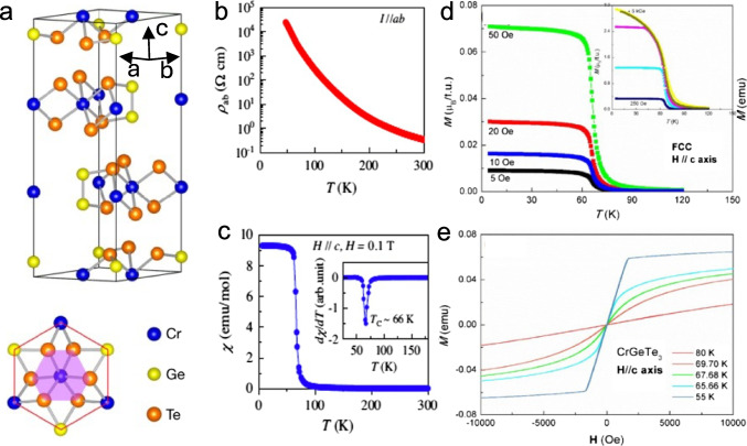
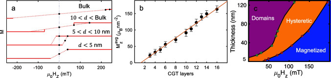
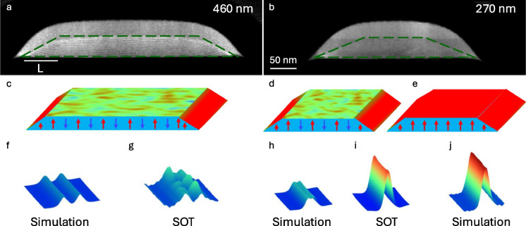
Van der Waals (vdW) ferromagnets have garnered extensive attention thanks to their layered structures and the possibility of thinning them down to just a few atomic layers. This review discusses the emergent nanoscale magnetism in CrGeTe₃ (CGT), a 2-D vdW ferromagnet, focusing on its nanoscale properties and potential spintronic applications. We report on local magnetic probe techniques showing that thin CGT films exhibit spontaneous global magnetization at zero field, while thicker flakes display a hard ferromagnetic response only at their edges. We then focus on magnetic edge states in CGT thin films and their potential applications, where direct amorphization of CGT results in magnetic edges similar to those in cleaved films. By fabricating nanopatterned magnetic arrays, it has been demonstrated that tunable magnetic states emerge with anomalous coercivity. Moreover, we present the potential to realize artificial spin-ice configurations through antiferromagnetic dipolar coupling. The review delves into CGT heterostructures, which have demonstrated an anomalous Hall effect, expanding the scope of phenomena accessible in thin magnets. Finally, we discuss observation of magnetic bubbles and skyrmions, which offer additional opportunities for exploring chiral domain structures. The studies of CGT underscore the promise of fundamental investigations into 2-D magnetism while opening new pathways for spintronic applications based on nanoscale magnetic effects and frustration phenomena.

Keywords: CrGeTe3; Magnetic imaging; Magnetism; Skirmion; Van der Waals materials.


Conflict of interest statement

Conflict of interestThe authors declare no competing interests.

Figures

Fig. 1
Fig. 1
CrGeTe3 (CGT) properties. a Crystal structure (side and top views) of CGT. Bulk CGT has a layered structure with interlayer vdW coupling (Cheng et al. [9]). b In-plane resistivity, ρab, as a function of temperature. c Zero field-cooled (ZFC) magnetic susceptibility χ at H=0.1 T applied along the c-axis. Inset: temperature derivative of dχdT. (Dilip et al. [29]). d, e SQUID measurements on bulk CGT of the magnetization dependence on temperature M–T for different magnetic fields (data for the highest fields shown in the inset) (d) and magnetic field M–H for different temperatures (Tengfei et al. [21])
Fig. 2
Fig. 2
Magnetic imaging of CrGeTe3 (CGT) from bulk to the 2-D limit. ad MFM images of the out-of-plane magnetic field dependence of magnetic domains. The sequence of images was obtained as it traversed various points of the magnetization vs. magnetic field (Yeonkyu et al. [20]). el Scanning SOT microscopy images Bz(x,y) of CGT at distinct values of applied out-of-plane field μ0Hz and sample thickness d=70 (eh) and 6 nm (il) (Noah et al. [22]). mp Scanning SOL images of CGT flake with 3 to 15 layers (Vervelaki et al. [25]). The blue and green dashed line in o represent layers with d = 4.9 and 11 nm (7 and 15 atomic layers), respectively. Image parameters: (ad) All MFM images were taken at 4.2 K with tip-sample distance of 400 nm. The scan size is 20×20μm2, with 128×128 pixels. μ0Hz= 0 (a), 100 (b), 240 (c), 0 mT (d). e–l SOT images (eh) d= 70 nm, area scan 5 × 5 µm2, pixel size 40 nm2. μ0Hz= 0 (e), 115 (f), 175 (g), 0 mT (h). i–l d= 6 nm, area scan 1 × 1 µm2, pixel size 30 nm2. μ0Hz= 0 (i), 20 (j), 120 (k), 0 mT (l). The blue to red color scale represents lower and higher magnetic field, respectively. mp SOL images: area scan 25×2 5 µm2. μ0Hz= 0 (e), 8 (f), 40 (g), 0 mT (h). The blue to red color scale represents lower and higher magnetic field, respectively
Fig. 3
Fig. 3
Bulk-to-thin film magnetization. a Sketched magnetization curves drawn from Bz(x,y) measured on film’s parts of different d. Dashed lines are a guide to the eye connecting the two saturated fields. The fields at which the images were taken are marked with black dots. b Mzavg plotted as a function of the CGT layers number and its corresponding linear fit shown with the red line (Vervelaki et al. [25]). c A thickness-dependent magnetization-state diagram of CGT shows three states: domains (purple), hysteretic (orange), and magnetized (blue)
Fig. 4
Fig. 4
Microscopy images of CrGeTe3 edges. a, b Sequence of natural cleaved CrGeTe3 (CGT) flakes acquired at μ0Hz= 0 mT after distinct field excursions to (a) Hexc<Hs-, (b) Hexc>Hs+. The blue and red edges represent the edge magnetization (Noah et al. [22]). c, d SOT images of FIB-patterned edges. The image acquired at μ0Hz=0 mT showing magnetic edges in nano-patterned CGT. e, f From 2-D to 1-D magnetic stripes. CGT patterned into stripes with varying effective widths (we) and length of 10 µm. e SEM image. f The SOT image acquired at μ0Hz=0 mT after positive field excursion. For stripes with w>wc, two distinct magnetized edges (red color scale) separated by a zero average magnetization in the stripe’s interior (color-coded in green). For stripes of width w<wc (rightmost stripe), the two edges appear to merge and form a single magnetic domain (Noah et al. [23]). Edge separation width from left to right: w=770,660,550,460,400, and 270 nm. Imaging parameters: a, b μ0Hz= 0 mT, area scan 3 × 3 µm2, pixel size 24 nm2. The blue to red color scale represents lower and higher magnetic field, respectively, with a shared scale for of Bz=1 mT. Imaging parameters: c, d μ0Hz= 0 mT, area scan 3×3 µm2 in size, pixel size 15 nm2, acquisition time 5 min/image. e μ0Hz= 0 mT, area scan 2.5×10 µm2, pixel size 40 nm2, acquisition time 5 min/image. The blue to red color scale represents lower and higher magnetic field, respectively
Fig. 5
Fig. 5
Average coercivity of CrGeTe3 (CGT) islands. ac Images of island arrays patterned via FIB with island dimensions d=60 nm for all arrays, and widths, w=1600 nm (a), 600 nm (b), and 150 nm (c). The nanoparticle characteristic size D determine the island magnetic state and coercivity. For islands with characteristic size larger than Ds as in a, w=1600 nm >Ds, the islands interior breaks to domain, while its edges are magnetized. b, c For islands with characteristic size smaller than Ds a single magnetic domain appears due to edge confinement. The images acquired near the coercive field of the corresponding arrays. d The median island coercive field, Hci (Hci~), as a function of the parameter w/V=1/wd (Noah et al. [24]). Imaging parameters: a μ0Hz= 70 mT, area scan 4.1×4.1 µm2, pixel size 32 nm2, b μ0Hz= 20 mT, area scan 11×11 µm2, pixel size 115 nm2, and (c) μ0Hz= 100 mT, area scan 4.2×4.2 µm2, pixel size 30 nm2. The scale bar is 1000 nm in all images. The black to white color scale represents lower and higher magnetic fields, respectively
Fig. 6
Fig. 6
Origin of the magnetic edge in CrGeTe3. a, b Scanning transmission electron microscope (STEM) cross-sectional images measured in the middle of the stripe (Fig. 4e) with effective widths we=460 nm (a) and we=270 nm (b). The effective crystalline CrGeTe3 (CGT) region is marked with green dashed lines. ce Schematic illustration of the local magnetic structure at the edges and interior for different stripe widths. In panels c and d, the edges but not the interior of the sample retain their magnetization. In panel e, the whole stripe is a hard ferromagnet. fj A comparison between the SOT images and magnetostatic simulations. f, h Simulations of the stripe magnetization resulting from the magnetized edges for a triangular cross-section, marked by red in panels c and d. j Simulations of the stripe magnetization assuming that the whole stripe is magnetized, marked by red in panel e. g, i Bz(x,y) SOT images of the stripes in a and b. The blue to red color scale represents lower and higher magnetic fields, respectively, with a shared scale of 3 mT (Noah et al. [23])
Fig. 7
Fig. 7
SOT image of CrGeTe3 terraces with a corresponding atomic force microscopy line scan. a, b SOT magnetic image at μ0Hz=200 mT (a), and μ0Hz=0 mT (b). The magnetic domains evolve with no relation to the step-edges. c Atomic force microscopy height profile measured along the black line presented in a resolving steps of ∼ 10 nm. Image parameters: area scan 5 × 5 μm2, pixel size 26 nm. The blue to red color scale represents lower and higher magnetic field, respectively, with a scale of Bz=1 mT (Noah et al. [22])
Fig. 8
Fig. 8
Separation dependent inter-island interactions. ad Sequence of binary matrices computed from the SQUID-on-tip (SOT) Bz(x,y) images for island separations of s=60 (a), 80 (b), 100 (c), and 200 nm (d) (islands thickness—d = 35 nm). The purple and gold lines delineate two fully anticorrelated sublattices. The black/white color scale represents the magnetic moments pointing down/up, and the gray represents amorphous CGT. The SOT images were acquired at the relevant coercive fields, μ0Hc= 68 (a), 89 (b), 99 (c), and 70 mT (d). e Illustration of matrices at the coercive field (MHz=Hc=0) with different types of inter-island correlations: A checkboard matrix that shows perfect anticorrelation with Moran’s I=-1 (left). A random matrix, which has zero spatial correlation I=0 (center). A perfectly correlated matrix for which I=1. f Gray: distribution of Moran’s I values calculated for random 9×9 matrices at the coercive field based on a set of 104 trials. Distinct markers represent the average Moran’s I measured for CGT arrays at Hc for separations of s=60 (black), 80 (blue), 100 (green), and 200(red) nm. The markers indicate the mean values, and the error bars the range within one standard deviation. I=0.00±0.08,-0.08±0.05,-0.16±0.08,and-0.25±0.1 for s=100,80, and 60 nm, respectively (Noah et al. [39])
Fig. 9
Fig. 9
Probing the anomalous Hall effect (AHE) in CrGeTe3 (CGT) heterostructures. a Optical micrograph of a Pt/CGT heterostructure with false color to clarify different regions of the device. False coloring is used to distinguish the different material layers: Pt (5 nm) in gray, CGT (30 nm) in green, Au in yellow, and SiO2 in dark red. b Anomalous Hall hysteresis loop in the Pt/CGT bilayer, measured at 4 K. Insets: MFM images of CGT acquired at different magnetic fields within the hysteretic state (Lohmann et al. [18]). c Optical image of a fabricated Hall bar device from a Ta/CGT heterostructure and measurement setup. d Normalized RAHE for CGT thicknesses of tCGT =50,38, and 8 nm. All three hysteretic curves exhibit similar AHE behavior (Ostwal et al. [17])
Fig. 10
Fig. 10
Magnetic bubbles in a CrGeTe3 (CGT) thin flakes. ad SOT images of magnetic bubbles in CGT. a, b Subsequent SOT images taken at μ0HZ=-90 and -95 mT. c Subtracting a, b SOT images with Δμ0HZ=5 mT resolve in magnetic bubble formation. d Subtracting two SOT images with Δμ0HZ=50 mT. ek Magnetic bubbles of different chirality in CGT. e, f Cryo-Lorentz transmission electron microscopy, transport of intensity equation (TIE)—reconstructed phase images of the same sample region after two different field-cooling experiments, showing a homochiral bubble lattice in e and a mixed-chirality bubble lattice in f. Bubbles with right-handed chirality are bright, and bubbles with left-handed chirality are dark. g, h Integrated magnetic induction maps of the green and orange boxes in (e, f) (chirality is indicated by red or blue arrow). i Phase image of a region of a CGT flake that has irregular topography. The right side of the sample is flat, and the left side is approaching a wrinkle in the flake. j, k Magnetic induction maps of the curved and flat regions, respectively (Artur et al. [26]). lr Skyrmionic spin texture in CGT. l, m Bzlever(x,y) maps of the thick part of the sample at μ0Hz=17 mT (l) and 28 mT (m), respectively, after field-cooling in 10 mT. nq Corresponding Bzx,yz and magnetization Mz(x,y) simulated at μ0Hz=26 (n, p) and 38 mT (o, q), showing stripe domains shrink into bubbles at higher field. r The simulated magnetization configuration of the magnetic bubbles at μ0Hz=38, showing a Bloch-type skyrmionic texture in the middle layer, which gradually transforms into a Néel-type texture at the surface layers (Vervelaki et al. [25])

References

    1. Zhang, W., Wong, P.K.J., Zhu, R., van der Wee, A.T.S.: Waals magnets: wonder building blocks for two-dimensional spintronics? InfoMat 1, 479–495 (2019)
    1. Jin, C., Kou, L.: Two-dimensional non-van der Waals magnetic layers: functional materials for potential device applications. J. Phys. D Appl. Phys. 54, 413001 (2021)
    1. Yang, S., Zhang, T., van der Jiang, C.: Waals magnets: material family, detection and modulation of magnetism, and perspective in spintronics. Adv. Sci. 8, 2002488 (2021) - PMC - PubMed
    1. Deng, Y., et al.: Layer–number-dependent magnetism and anomalous Hall effect in van der Waals ferromagnet Fe 5 GeTe 2. Nano Lett. 22, 9839–9846 (2022) - PubMed
    1. Thiel, L., et al.: Probing magnetism in 2D materials at the nanoscale with single-spin microscopy. Science 1979(364), 973–976 (2019) - PubMed

LinkOut - more resources