. 2025 Jul 1;16(1):6053.
doi: 10.1038/s41467-025-61085-6.

Ultrapure and efficient electroluminescence in alkali metal doped inorganic perovskite quantum wires arrays

Affiliations

Ultrapure and efficient electroluminescence in alkali metal doped inorganic perovskite quantum wires arrays

Yang Bryan Cao et al. Nat Commun. .

Abstract

Alkali metal doping has been widely utilized to regulate metal halide perovskites and improve their luminescence performance. However, due to the discordant tolerance factor caused by the smaller size of potassium and rubidium ions, it is still debatable whether they can be incorporated in the cesium perovskite crystal lattice. Here we provide unambiguous evidence for the formation of Rb+ and K+ substitutionally doped stable perovskite cubic crystal structure in the form of quantum wires embedded in nanoporous alumina template. The suppressed inner defects and enhanced exciton binding energy lead to a reduced non-radiative recombination in the co-doped perovskite quantum wires. The perovskite light-emitting diodes with a maximum external quantum efficiency of 17.5%, 21.2%, 24.9% and 30.1% and a maximum luminance of 1638 cd m-2, 3365 cd m-2, 13,483 cd m-2 and 31,706 cd m-2 for electroluminescence peak of 476 nm (primary-blue), 483 nm (sky-blue), 490 nm (sky-blue) and 512 nm (green) are fabricated respectively. Surprisingly, all devices emit high-color purity light with narrow linewidth of ≤16 nm.


Conflict of interest statement

Competing interests: The authors declare no competing interests.

Figures

Fig. 1
Fig. 1. Substitution of Cs with Rb and K at A-site in alkali metals doped PeQW arrays.
a Schematic illustration of the fabrication of alkali metals doped PeQW arrays and substitution of Cs with Rb and K at A-site in PeQW. Inset, cross-sectional TEM image of PeQW arrays. Scale bar, 200 nm. b Atomically resolved low-dose HRTEM image of single pristine CsPbBr3 QW with atomic structure model projected along <100> direction. Scale bar, 2 nm. Inset, fast Fourier transform diffractograms showing the cubic lattice structure. Scale bar, 2 nm−1. c, d Zoom-in low-dose HRTEM image of perovskite lattice in the edge and middle of pristine CsPbBr3 QW. Scale bar, 1 nm. e Rb 3 d and K 2p XPS core-level spectra of Rb+, K+: CsPbBr3 QWs. f XRD pattern of pristine CsPbBr3 QW, Rb+: CsPbBr3 QWs and Rb+, K+: CsPbBr3 QWs. g GIWAXS pattern and in-plane intensity profiles extracted from the GIWAXS of pristine CsPbBr3 QW, Rb+: CsPbBr3 QWs and Rb+, K+: CsPbBr3 QWs. h Atomically resolved low-dose HRTEM image of single pristine CsPbBr3 QW with atomic structure model projected along <110> direction. Scale bar, 2 nm. Inset, fast Fourier transform diffractograms showing the cubic lattice structure. Scale bar, 5 nm−1. i, j Zoom-in low-dose HRTEM image of perovskite lattice in the edge and middle of Rb+, K+: CsPbBr3 QWs. Scale bar, 1 nm.
Fig. 2
Fig. 2. DFT calculation of formation energy for the substitution of Cs with Rb and K at A-site.
a Schematic drawing of Rb or K replacing Cs at A-site in the model without Al2O3. b Formation energy of Rb or K replacing Cs at A-site. c Schematic drawing of Rb or K replacing Cs at A-site in the model with Al2O3. d Formation energy of Rb or K replacing Cs at A-site in the bulk of CsPbBr3. e Formation energy of Rb or K replacing Cs at A-site at the interface of CsPbBr3 and Al2O3.
Fig. 3
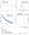
Fig. 3. Properties of alkali metals doped PeQW arrays.
a XRD patterns, b Normalized photoluminescence spectra (λex=350nm), c TRPL decay curves and d PLQYs (λex=365nm) measured at corresponding photoluminescence peak of as-synthesized alkali metals doped PeQWs. e Environmental photoluminescence stability under ambient condition for alkali metal doped PeQWs.
Fig. 4
Fig. 4. Characteristics of PeLEDs based on alkali metals doped PeQW arrays.
a Schematic of alkali metals doped PeQWs-based LED architecture. b Cross-sectional SEM image of a device. The thickness of each layer, which can be confirmed by SEM, are shown below: Al electrode/Al2O3 hole blocking layer (~5 nm)/PeQWs emission layer (90 nm)/TAPC hole transporting layer (20 nm)/HAT-CN hole injecting layer (20 nm)/ITO transparent electrode (90 nm). Scale bar, 200 nm. c Energy band diagram of each layer in PeLEDs. d Normalized electroluminescence spectra of blue and green PeLEDs. e The corresponding CIE coordinates of blue and green PeLEDs. f Current density (J)-voltage (V)-luminance (L) curves. g, h External quantum efficiency (EQE)-luminance (L) curves. i The EQEs distribution collected from 72 devices. The average peak EQEs are 15.8%, 18.2%, 20.2% and 26.2% with relative standard deviations of 7.7%, 7.3%, 11.1% and 7.3%, respectively.

Similar articles

References

    1. Saliba, M. et al. Incorporation of rubidium cations into perovskite solar cells improves photovoltaic performance. Science354, 206–209 (2016). - PubMed
    1. Abdi-Jalebi, M. et al. Maximizing and stabilizing luminescence from halide perovskites with potassium passivation. Nature555, 497–501 (2018). - PubMed
    1. Kausar, A. et al. Advent of alkali metal doping: a roadmap for the evolution of perovskite solar cells. Chem. Soc. Rev.50, 2696–2736 (2021). - PubMed
    1. Li, Y. -h. et al. Review on the promising roles of alkali metals toward highly efficient perovskite light-emitting diodes. J. Mater. Chem. C.11, 2011–2025 (2023).
    1. Wang, Z. et al. Suppressed phase segregation for triple-junction perovskite solar cells. Nature618, 74–79 (2023). - PubMed

LinkOut - more resources