. 2025 Jul 7;14(1):238.
doi: 10.1038/s41377-025-01832-y.

On-chip graphene photodetectors with a nonvolatile p-i-n homojunction

Affiliations

On-chip graphene photodetectors with a nonvolatile p-i-n homojunction

Ruijuan Tian et al. Light Sci Appl. .

Abstract

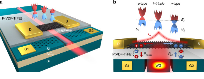
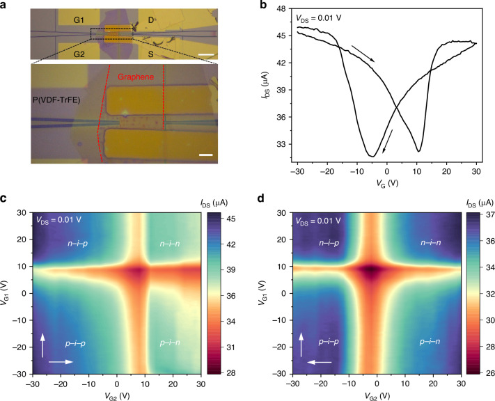
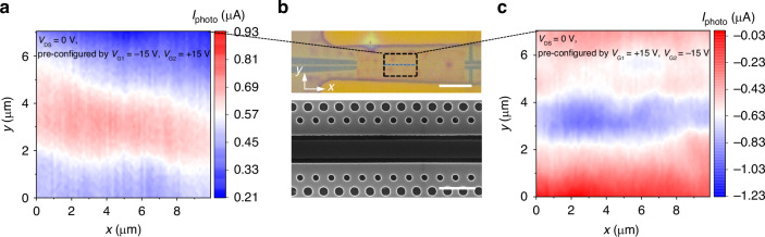
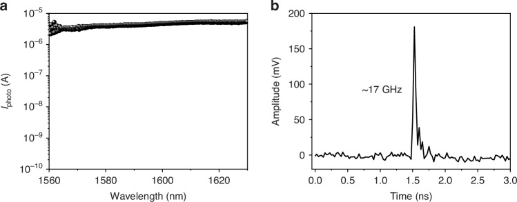
Graphene's unique photothermoelectric (PTE) effect, combined with its compatibility for on-chip fabrication, promises its development in chip-integrated photodetectors with ultralow dark-current and ultrafast speed. Previous designs of on-chip graphene photodetectors required external electrical biases or gate voltages to separate photocarriers, leading to increased power consumption and complex circuitry. Here, we demonstrate a nonvolatile graphene p-i-n homojunction constructed on a silicon photonic crystal waveguide, which facilitates PTE-based photodetection without the need for electrical bias or gate voltages. By designing an air-slotted photonic crystal waveguide as two individual silicon back gates and employing ferroelectric dielectrics with remnant polarization fields, the nonvolatile p-i-n homojunction with a clear gradient of Seebeck coefficient is electrically configured. Hot carriers in the graphene channel generated from the absorption of waveguide evanescent field are separated by the nonvolatile p-i-n homojunction effectively to yield considerable photocurrents. With zero-bias and zero-gate voltage, the nonvolatile graphene p-i-n homojunction photodetector integrated on the optical waveguide exhibits high and flat responsivity of 193 mA W-1 over the broadband wavelength range of 1560-1630 nm and an ultrafast dynamics bandwidth of 17 GHz measured in the limits of our instruments. With the high-performance on-chip photodetection, the nonvolatile graphene homojunction directly constructed on silicon photonic circuits promises the extended on-chip functions of the optoelectronic synapse, in-memory sensing and computing, and neuromorphic computing.


Conflict of interest statement

Conflict of interest: The authors declare no competing interests.

Figures

Fig. 1
Fig. 1. Schematic of the waveguide-integrated nonvolatile graphene pin homojunction photodetector.
a Schematic of the graphene pi–n homojunction photodetector constructed on a PC waveguide with two air slots, showing optical mode propagating in the central waveguide and two separated back gates provided by the silicon PC slab with the P(VDF-TrFE) dielectric layer. b Gradients of Seebeck coefficient (ΔS) and hot-carrier temperature (Te) over the nonvolatile graphene p–i–n homojunction. A downward (upward) polarization field Pdown (Pup) of the P(VDF-TrFE) layer causes the graphene layer to be doped in p−type (n−type). Different doping levels of graphene gated by air-slotted PC waveguide result in the gradient of Seebeck coefficient ΔS = S1S2. The Fermi level of graphene is also provided for guiding the Seebeck coefficient variations related to the doping of graphene along the channel. Hot-carrier temperature Te distributions of the graphene layer correspond to the guiding mode in the PC waveguide
Fig. 2
Fig. 2. Electrical characteristics of nonvolatile graphene pin homojunction constructed on the air-slotted silicon PC waveguide with the dielectric layer of P(VDF-TrFE).
a Top panel: optical microscope image of a fabricated device. Scale bar, 50 μm. Bottom panel: the zoomed image of the active section of the device, consisting of graphene flake and P(VDF-TrFE) coated on the PC waveguide substrate. Scale bar, 10 μm. b Transfer curve of the graphene channel with the global gate voltages VG = VG1 = VG2, and VDS = 0.01 V. c Source-drain current IDS map at VDS = 0.01 V with varying VG1 from 30 V to 30 V, VG2 from 30 V to 30 V. d Source-drain current IDS map at VDS = 0.01 V with varying VG1 from 30 V to 30 V, VG2 from 30 V to 30 V, as indicated by the white arrows
Fig. 3
Fig. 3. Spatially resolved photocurrent distribution of nonvolatile graphene pin homojunction constructed on the air-slotted silicon PC waveguide with the dielectric layer of P(VDF-TrFE).
a Scanning photocurrent map of the graphene pin junction at VDS = 0 V after a programming pulse gate voltage of VG1 = −15 V, VG2 = +15 V. b The corresponding scanning region is outlined by the black dashed line in the top panel. Scale bar, 10 μm. A zoomed view of the PC waveguide captured a part of the outlined region in the optical image of the top panel is shown in the bottom panel. Scale bar, 1 μm. c Scanning photocurrent map of the graphene nip junction at VDS = 0 V after a programming pulse gate voltage of VG1 = +15 V, VG2 = −15 V
Fig. 4
Fig. 4. Steady-state photoresponses of the nonvolatile graphene pin homojunction integrated on silicon PC waveguide with a laser at 1620 nm guided in the waveguide.
a Measured photocurrent map at zero bias after the configurations with different gate voltages on G1 and G2. b Optical power dependence of the photocurrents at VDS = 0 V after pulsed gate voltages of VG1 = −15 V and VG2 = +15 V to configure the graphene pi–n homojunction. c Monitored photocurrents for 28 h after the removal of the gate voltages, displaying excellent endurance and retention performance
Fig. 5
Fig. 5. Wavelength-dependent and high-speed photoresponse of the waveguide-integrated nonvolatile graphene pin homojunction photodetector at zero-bias after the configuration of VG1 = −15 V and VG2 = +15 V.
a Wavelength-dependent photocurrent ranging from 1560 to 1630 nm. b Measured impulse response, showing a 3 dB bandwidth of 17 GHz limited by the employed oscilloscope

Similar articles

References

    1. Romagnoli, M. et al. Graphene-based integrated photonics for next-generation datacom and telecom. Nat. Rev. Mater.3, 392–414 (2018).
    1. Wu, G. J. et al. Programmable transition metal dichalcogenide homojunctions controlled by nonvolatile ferroelectric domains. Nat. Electron.3, 43–50 (2020).
    1. Zhou, Z. C. et al. Prospects and applications of on-chip lasers. eLight3, 1 (2023). - PMC - PubMed
    1. Lipson, M. The revolution of silicon photonics. Nat. Mater.21, 974–975 (2022). - PubMed
    1. Shastri, B. J. et al. Photonics for artificial intelligence and neuromorphic computing. Nat. Photonics15, 102–114 (2021).

LinkOut - more resources