Review
. 2025 Jul 4;18(13):3175.
doi: 10.3390/ma18133175.

Thin-Film Encapsulation for OLEDs and Its Advances: Toward Engineering

Affiliations
Review

Thin-Film Encapsulation for OLEDs and Its Advances: Toward Engineering

Songju Li et al. Materials (Basel). .

Abstract

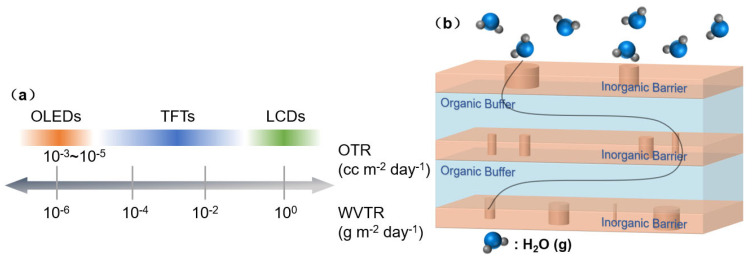
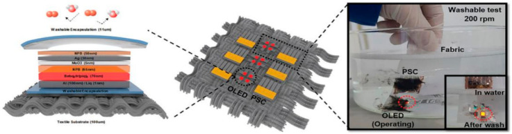
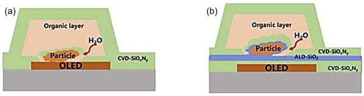
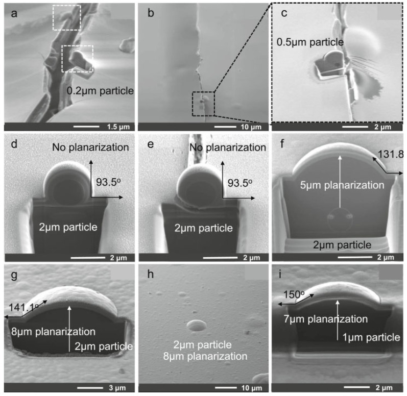
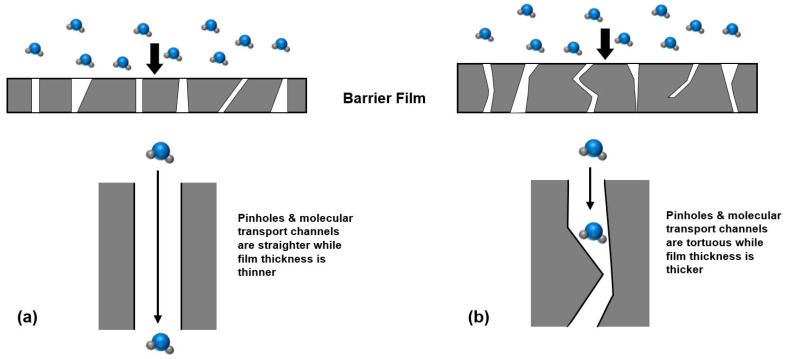
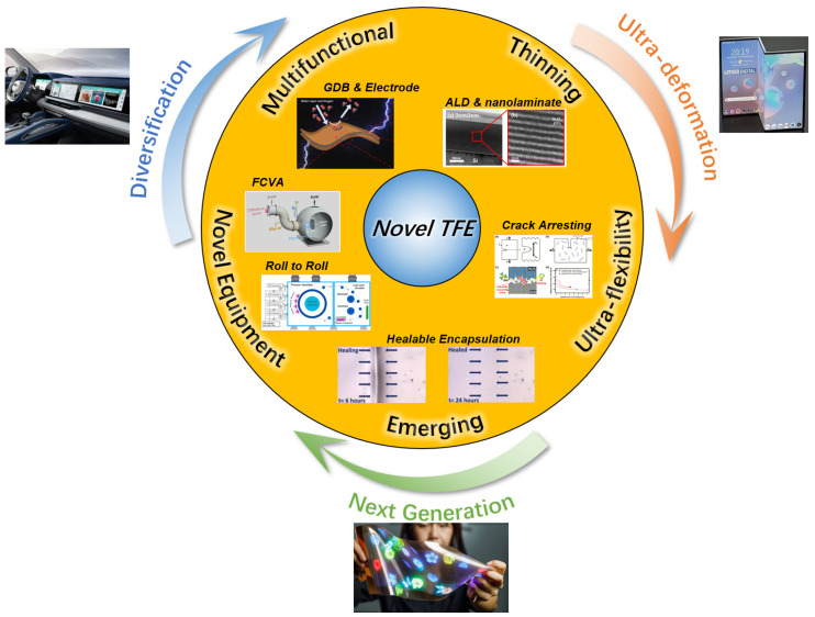
Thin-film encapsulation has been a critical method to realize small-size OLED displays. However, the manufacturing of large-size flexible OLED is still in the preparatory phase prior to commercialization, which entails more rigorous demands for reliability and flexibility with regard to thin-film encapsulation. This review, from the perspective of engineering for mass production, addresses the development of thin-film encapsulation and its three core properties for comprehensive validation while engineering, including basic properties, reliability, and compatibility. Moreover, considering the prospective evolution of display products, the review on novel thin-film encapsulation was conducted to evaluate the potential engineering value for thinning, ultra-flexibility, multifunctionality, novel equipment, and emerging technology. It is anticipated that some of the aforementioned technologies may prove to be of significant engineering value. It is therefore hoped that by comprehensive engineering verification, the commercial application of novel thin-film encapsulation can be promoted and the competitiveness of OLED products can be effectively enhanced.

Keywords: engineering; large-size OLEDs; multifunctionality; thin-film encapsulation; thinning; ultra-flexibility.


Conflict of interest statement

Authors Songju Li, Zhuo Gao, Xiaolin Yan, Dong Fu and Xianwen Sun were employed by the company Guangdong Juhua Printed Display Technology Co., Ltd. Author Min Li was employed by the company Guangzhou New Vision Optoelectronic Co., Ltd. The remaining authors declare that the research was conducted in the absence of any commercial or financial relationships that could be construed as a potential conflict of interest.

Figures

Figure 1
Figure 1
(a) Requirement of WVTR for different devices. (b) Schematic mechanism for increasing water vapor intrusion pathways.
Figure 2
Figure 2
Simple classification and development path of OLED encapsulation technology.
Figure 3
Figure 3
Items of property for the complete functioning of TFE while engineering.
Figure 4
Figure 4
(af) Peeling phenomenon caused by large stress (copyright © 2016, American Chemical Society).
Figure 5
Figure 5
Schematic diagram of the principle of counteracting the opposite-direction stress and its resultant figure.
Figure 6
Figure 6
Schematic illustration of the principle of MLD organic layers for buffering thermal expansion coefficient mismatches (copyright © 2013, American Chemical Society).
Figure 7
Figure 7
SEM schematics of SiOxNy films with oxygen compositions of (a) 0.08; (b) 0.10; (c) 0.47; and (d) 1.13, respectively, that produced cracks after bending. The left column of images shows the top view, and the middle and right columns of images show the cross-sectional view and its enlarged view (copyright © 2016, Elsevier B.V. All rights reserved.).
Figure 8
Figure 8
Schematic structure of a microlens on TFE.
Figure 9
Figure 9
Schematic structure of a fabric display.
Figure 10
Figure 10
Schematic representation of (a) the effect of particles on TFE and (b) the role of ALD-SiO2 used to cover the particles.
Figure 11
Figure 11
Cross-sectional SEM images of (ae) generation of cracks around particles of different sizes after bending and (fi) larger particles that can also be passivated after bending with the addition of a planarization layer [39].
Figure 12
Figure 12
Schematic representation of (a) straight channels and (b) tortuous channels for molecular transportation.
Figure 13
Figure 13
(a) Cross-sectional SEM image representing particle resulting in the formation of water vapor intrusion channel in the encapsulation film [16] (copyright © 2023, The Society for Information Display). (b) Schematic diagram of flattening performance evaluation method.
Figure 14
Figure 14
Relation between thin film thickness and critical strain [91] (copyright © 2015, American Chemical Society).
Figure 15
Figure 15
SEM image representing bulge of Al2O3 thin film at compressive strain.
Figure 16
Figure 16
Cross-sectional SEM image of peeling due to low adhesion (copyright © 2019, The Society for Information Display).
Figure 17
Figure 17
(a,b) Schematic of edge failure of OLED display after high-temperature and high-humidity storage test. (c) Plot of lateral distance between the edge of the encapsulation and the OLED active area versus the time to failure (copyright © 2019, The Society for Information Display).
Figure 18
Figure 18
(a) Traditional TFE edge structure. (b) Optimized TFE edge structure for inhibition of crack propagation utilizing organic-layer block.
Figure 19
Figure 19
An overview of novel TFE technologies in terms of thinning, ultra-flexibility, novel equipment, multifunctional, and emerging technologies. Each technology is driven by the corresponding product type.
Figure 20
Figure 20
Schematic representation of the demand for TFE thinning in high-resolution OLED displays.
Figure 21
Figure 21
Schematic diagram of the growth process of commonly used ALD (Al2O3).
Figure 22
Figure 22
Schematic diagram of (a) ALD-AlOx hydrolysis mechanism; (b) APP treatment for ALD Al2O3 (copyright © 2021, American Chemical Society); (c) AFM and SEM images for demonstration of ALD-monolayer and ALD-nanolaminate after RA test (copyright © 2014, American Chemical Society); (d) cross-sectional TEM images for illustration of ALD-Al2O3/ALD-ZrO2 nanolaminate [105] (copyright © 2013 Elsevier B.V. All rights reserved).
Figure 23
Figure 23
(a,b) Schematic of the passivation mechanism of natural microcracks against mechanically induced cracks; (c) microcracks in Al2O3/ZnO/MgO nanolaminates and their mechanism of function: microcracks generated by the corrosion of ZnO during the deposition of Al2O3 develop centers to trap and buffer the cracks (copyright © 2017, American Chemical Society); (d,e) encapsulation performance of Al2O3 with S-H organic layer and its reliability performance under 60 °C/90% R.H. environment for OLED displays (copyright © 2013, Elsevier B.V. All rights reserved).
Figure 24
Figure 24
(a) Schematic diagram and TEM image of plasma polymer and ALD-Al2O3 nanolaminate. (b) Plot of the relationship between the number of nanolaminates and the barrier property [138] (copyright © 2017, American Chemical Society). (c) Schematic diagram of the formation of organic/inorganic stacks of MLD-SALOs and ALD-Al2O3, with (d) plot of the reliability test results of OLEDs encapsulated with MLD/ALD stacked structure (copyright © 2017, American Chemical Society).
Figure 25
Figure 25
(a) Schematic diagram of ALI principle; (b) schematic diagram of PMMA fluorination treatment to form a structure contributing to bending reliability (copyright © 2021, Elsevier B.V. All rights reserved); (c) schematic diagram of the mechanism of 2D material to enhance the reliability and comparison of AFM before and after passivation of defects [122] (copyright © 2017, Elsevier Ltd. All rights reserved); (d) schematic diagram of the thermal stress presetting and its counteracting mechanism (copyright © 2022, Elsevier B.V. All rights reserved).
Figure 26
Figure 26
Schematic application of (a) angle-selectable layer, (b) optical support layer (copyright © 2020, American Chemical Society), and (c) wrinkle layer (copyright © 2019, The Korean Society of Industrial and Engineering Chemistry, Published by Elsevier B.V. All rights reserved).
Figure 27
Figure 27
Multifunctionalities of TFEs in terms of (a,b) electric and (c) chemical tolerance (copyright © 2018, American Chemical Society; © 2017, American Chemical Society; and © 2013, Royal Society of Chemistry, respectively).
Figure 28
Figure 28
(a,b) Schematic diagrams of the composition of multifunctional gas diffusion multibarrier and the structure of the fabric display; (c) illustration of the encapsulation of the fabric display and the performance of the UV light attenuation; (d,e) schematic diagrams of the preparation and working principle of the self-healing barrier; (f,g) illustration of the repair performance of the self-healing barrier (copyright © 2023, Wiley-VCH GmbH).
Figure 29
Figure 29
(ac) Schematic diagrams of the fabrication and mechanism of PONT and (d,e) illustrations showing its encapsulation performance.
Figure 30
Figure 30
Schematic diagrams of apparatus including (a) spatial ALD [43] (copyright © 2017, American Chemical Society) [160], (b) UV-ALD (copyright © 2021, Elsevier B.V. All rights reserved), (c) FCVA (copyright © 2022, Elsevier Ltd. All rights reserved), (d) iCVD + ALD (copyright © 2022, Wiley-VCH GmbH), and (e) R2R (copyright © 2021, Published by Elsevier Ltd.).

Similar articles

References

    1. Adachi C., Nagai K., Tamoto N. Molecular design of hole transport materials for obtaining high durability in organic electroluminescent diodes. Appl. Phys. Lett. 1995;66:2679–2681. doi: 10.1063/1.113123. - DOI
    1. Reineke S., Lindner F., Schwartz G., Seidler N., Walzer K., Lüssem B., Leo K. White organic light-emitting diodes with fluorescent tube efficiency. Nature. 2009;459:234–238. doi: 10.1038/nature08003. - DOI - PubMed
    1. Xu R.-P., Li Y.-Q., Tang J.-X. Recent advances in flexible organic light-emitting diodes. J. Mater. Chem. C. 2016;4:9116–9142. doi: 10.1039/C6TC03230C. - DOI
    1. Li Y., He P., Chen S., Lan L., Dai X., Peng J. Inkjet-Printed Oxide Thin-Film Transistors Based on Nanopore-Free Aqueous-Processed Dielectric for Active-Matrix Quantum-Dot Light-Emitting Diode Displays. ACS Appl. Mater. Interfaces. 2019;11:28052–28059. doi: 10.1021/acsami.9b08258. - DOI - PubMed
    1. He P., Lan L., Deng C., Wang J., Peng J., Cao Y. Highly efficient and stable hybrid quantum-dot light-emitting field-effect transistors. Mater. Horiz. 2020;7:2439–2449. doi: 10.1039/D0MH00951B. - DOI

LinkOut - more resources