

Defect Density Analysis of WO x and MoO x Thin Films Grown by Pulsed Laser Deposition for Heterojunction Solar Cell Applications
- PMID: 40677973
- PMCID: PMC12264978
- DOI: 10.1021/acsaem.5c00629
Defect Density Analysis of WO x and MoO x Thin Films Grown by Pulsed Laser Deposition for Heterojunction Solar Cell Applications
Abstract
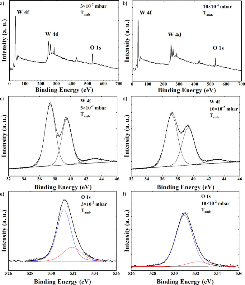
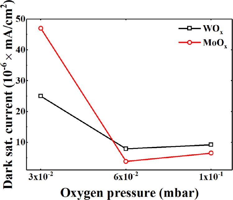
This study presents a comprehensive analysis of the optical and electronic properties of thin films of molybdenum oxide and tungsten oxide to implement hole-selective contact for heterojunction solar cells. These contacts are currently viewed as an alternative for the fabrication of doping-free solar cells. However, the spreading of this technology is still limited due to the development of S-shaped J-V curves, which affect the electrical performance of the cells, and further optimization in the material deposition process is therefore crucial to overcome these challenges. To improve transition metal oxide-based heterojunction technology, this work investigates the impact of oxygen vacancies on electrical performance, particularly their role in S-shaped J-V curves. Defect density evaluation through nondestructive techniques like photothermal deflection spectroscopy together with a detailed experimental characterization is presented in this paper to highlight the structural and optical properties of the films. Prototypes of solar cells incorporating hole-selective contacts with tungsten and molybdenum oxide are prepared to show S-shaped J-V characteristics under AM 1.5 illumination. An equivalent circuit modeling was used for understanding the electrical characteristics of the prototypes. Furthermore, this approach offers insights into the optimization of the performances of devices.
Keywords: defect density; heterojunction solar cells; molybdenum oxide; photothermal deflection spectroscopy; pulsed laser deposition; transition metal oxides; tungsten oxide.
© 2025 The Authors. Published by American Chemical Society.
Figures


References
-
- Simon Philipps; Werner Warmuth. Photovoltaics Report; Freiburg, 2024. https://www.ise.fraunhofer.de/content/dam/ise/de/documents/publications/.... accessed 18 April 2025.
-
- International Technology for Photovoltaics (ITRPV), Sixteenth Edition; 2025. https://www.vdma.org/international-technology-roadmap-photovoltaic. accessed 18 April 2025.
-
- LONGi. LONGi Sets New World-Record for Silicon Solar Cell Efficiency, Launching 2nd Generation Ultra-Efficient BC-Based Module https://www.longi.com/en/news/longi-hi-mo9-bc-world-record/. accessed 19 April 2025.
-
- Green M. A., Dunlop E. D., Yoshita M., Kopidakis N., Bothe K., Siefer G., Hao X.. Solar Cell Efficiency Tables (Version 63) Prog. Photovolt: Res. Appl. 2024;32(1):3. doi: 10.1002/pip.3750. - DOI
LinkOut - more resources
Full Text Sources