. 2025;21(7):1106-1111.
doi: 10.1038/s41567-025-02899-5. Epub 2025 May 21.

Valley-controlled photoswitching of metal-insulator nanotextures

Affiliations

Valley-controlled photoswitching of metal-insulator nanotextures

Hannes Böckmann et al. Nat Phys. 2025.

Abstract

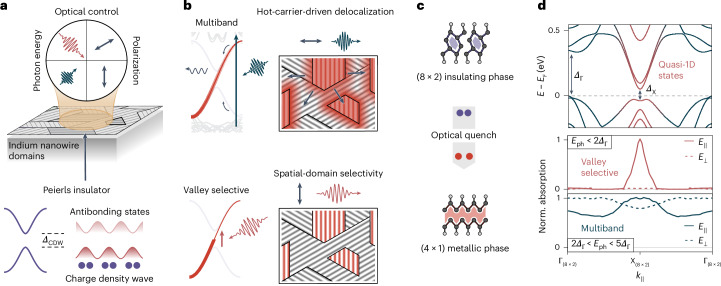
Spatial heterogeneity and phase competition are hallmarks of strongly correlated materials, influencing phenomena such as colossal magnetoresistance and high-temperature superconductivity. Active control over phase textures further promises tunable functionality at the nanoscale. Although light-induced switching of a correlated insulator to a metallic state is well established, optical excitation generally lacks the specificity to select subwavelength domains and determine final textures. Here we drive the domain-specific quench of a textured Peierls insulator using valley-selective photodoping. Polarized excitation exploits the anisotropy of quasi-one-dimensional states at the charge-density-wave gap to initiate an insulator-metal transition with minimal electronic heating. We find that averting dissipation facilitates domain-specific carrier confinement, control over nanotextured phases and reduction in thermal relaxation from the metastable metallic state. This valley-selective photoexcitation approach will enable the activation of electronic phase separation beyond thermodynamic limitations, facilitating optically controlled hidden states, engineered heterostructures and polarization-sensitive percolation networks.

Keywords: Electronic properties and materials; Nanowires; Phase transitions and critical phenomena; Surfaces, interfaces and thin films.


Conflict of interest statement

Competing interestsThe authors declare no competing interests.

Figures

Fig. 1
Fig. 1. Optical surface electronic texture control via valley-selective photodoping.
a, Top: schematic of the optical control parameters that drive selective surface domain switching. Bottom: the Peierls transition in a 1D atomic chain yields the formation of a periodic lattice distortion and CDW with a characteristic energy gap (ΔCDW). The electron density of valence (dark red) and conduction (light red) states exhibits a bonding and antibonding character with respect to the CDW along the chain direction. b, Top: light-induced electronic quench of the CDW phase. A population of states at the CDW gap, mediated by higher-lying surface bands (Multiband), is accompanied by electronic and lattice heating and yields a homogeneous phase change across the surface via delocalized energetic charge carriers. Bottom: direct bandgap excitation (Valley selective) minimizes dissipation, which manifests in domain-specific switching (red wires), with pronounced phase coexistence and local carrier confinement. c, Optical transition between the insulating (8 × 2) and metallic (4 × 1) phases of indium nanowires. d, Top: density-functional-theory-calculated electronic band structure of the Si(111) (8 × 2)–In phase (Methods). ΔΓ and ΔX denote the direct bandgaps, leading to the formation of energetic valleys in the band structure. Bottom: energy-integrated optical absorption. X-valley selectivity for low excitation energies and parallel polarization minimizes electronic heating and enables orientation-specific switching. Unspecific multiband absorption at higher excitation energies yields a delocalized hot-carrier distribution and homogeneous switching. The threshold energy is chosen to illustrate the transition between the regimes (see also Supplementary Fig. 1). k is the momentum vector along the Brillouin-zone high-symmetry points with respect to the wire direction.
Fig. 2
Fig. 2. Polarization and photon energy dependencies of the (8 × 2) to (4 × 1) switching efficiency.
a, LEED image and real-space sketch of parallel-oriented indium atomic wires on a stepped Si wafer surface with a 2° miscut relative to the (111) plane. b, Polarization-dependent switching efficiency for increasing photon energy, at the maximum diffraction spot suppression (1 – I(8 × 2)Δt = 40 ps/I(8 × 2)Δt = −150 ps). The in-plane electric-field component is depicted relative to the nanowire direction. Incident fluences (from left to right): 1.04 mJ cm–2, 0.59 mJ cm–2, 0.62 mJ cm–2, 1.09 mJ cm–2 and 1.40 mJ cm–2.
Fig. 3
Fig. 3. Polarization-sensitive and charge-transfer-induced switching in a domain texture.
a, Three-fold symmetric rotational domains on a flat Si(111) wafer surface. The LEED image comprises a superposition of domain-specific reflexes. b, Polarization-dependent switching of rotational domains. Δφ denotes the angle between the in-plane electric field and the nanowire orientation. c, Isotropic switching at near-IR wavelengths for all domain orientations in the entire fluence range. d, Transition between valley-selective to multiband excitation manifests in a loss of the intrinsic anisotropy (Fig. 2) due to the interdomain transfer of hot charge carriers. Incident fluences for 0.8 eV, 1.2 eV and 1.55 eV are 1.60 mJ cm–2, 1.40 mJ cm–2 and 2.03 mJ cm−2, respectively.
Fig. 4
Fig. 4. Lattice heating and thermal relaxation of the metastable (4 × 1) phase, driven by optical excess energy.
a, Integrated (8 × 2) diffraction spot intensity as function of pump–probe delay Δt at incident photon energies of 0.8 eV and 1.55 eV on a stepped wafer. The light polarization was chosen parallel and perpendicular to the nanowire orientation, respectively, corresponding to the maximum switching efficiency at fluences of F0.8 = 1.95 mJ cm−2 and F1.55 = 3.12 mJ cm−2. For identical intensity suppression, the relaxation into the (8 × 2) ground state accelerates with photon energy due to increasing thermal lattice fluctuations, following the phase transition (see the inset). b, Corresponding (4 × 1) diffraction spot intensity. Increased lattice heating at 1.55-eV excitation manifests in an intensity reduction due to the Debye–Waller effect (ΔIDBW). c, Pump-induced dynamic disorder increases the diffuse background intensity, counteracted by a reduction in the static disorder from enhanced phase homogeneity. d, Left: real-space sketch of indium atomic wires in the (8 × 2) phase, showing characteristic phase defects (alongside phase boundaries), which cause diffuse background scattering. Right: the photoinduced (4 × 1) structure exhibits an increased phase homogeneity. Thermal lattice fluctuations cause an accelerated relaxation for increasing photon energy.
Extended Data Fig. 1
Extended Data Fig. 1. Experimental setup of ultrafast LEED.
Ultrashort electron pulses, photoemitted from an electron gun, probe the microscopic surface structure after pump-probe delay Δt. The optical quench of the structural distortion manifests in a loss/gain of (8 × 2)/(4 × 1) reflex intensity.
Extended Data Fig. 2
Extended Data Fig. 2. Analyzed diffraction features.
Schematic diffraction image of the (8 × 2) indium phase on the (111) face of a Si wafer. (8 × 2) diffraction spots, analyzed in Fig. 2 on a stepped wafer (a) and in Fig. 3 on a flat wafer (b) are highlighted (blue). c, (8 × 2) (blue), (4 × 1) (red) and diffuse background (green) features, analyzed in Fig. 4.
Extended Data Fig. 3
Extended Data Fig. 3. Band structure and valley-selective photoexcitation.
Left, density-functional-theory (DFT) calculated electronic band structure of the Si(111)(8 × 2)-In phase (see Methods for details). Gray, projected Si bulk bands; dark green, surface localized bands; red, quasi-1D states with bonding and anti-bonding orbital character (right). ΔΓ and ΔX denote CDW gaps, leading to the formation of energetic valleys in the band structure. k∣∣ and k are the momentum vectors along Brillouin zone high-symmetry points with respect to the wire direction.
Extended Data Fig. 4
Extended Data Fig. 4. Predicted functionality of an optically switchable percolation network.
a, Measured rotational domain-resolved surface area fraction, switched into the (4 × 1) phase at 0.8 eV photon energy (see also Fig. 3b). The insets indicate particularly domain-selective optical polarization states. b, Proposed optical steering of electronic transport in a percolated domain texture within a Hall bar geometry. Red, metallic (4 × 1); blue, insulating (8 × 2) domains. Based on the anisotropic conductivity of indium atomic chains, selective domain switching could be used to control the transversal charge flow within the metallic percolation network. c, Top, calculated anisotropy along the conducting network principal axes with incident polarization, using experimental data. The anisotropy in resistance along the principal axes is peaked when one orientation is deselected by choosing a polarization perpendicular to the wire direction. In this scenario, the preferential transport along the wire direction yields a lateral deflection of charge carriers, resulting in a transversal voltage with tunable polarity. Bottom, transversal to longitudinal voltage ratio across the Hall bar. The voltage polarity can be optically switched by deselecting individual wire orientations.
Extended Data Fig. 5
Extended Data Fig. 5. Tight-binding calculation of Peierls heterostructure local density of states.
a, Sketch of transient quantum well formation due to suppressed relaxation dynamics and domain-specific switching. Long-lived metallic segments are embedded in relaxed insulating nanowires. b, Tight-binding calculations of the local density of states along the atomic chain show the formation of quantized metallic states within the insulating band gap (ΔX). In the transition region one expects strong band bending and therefore high curvature, which increases the effective mass of the electron and causes localization. Mismatch in band alignment between the metallic and insulating phase further leads to confinement even beyond the insulating gap in metallic and insulating segments.

References

    1. de la Torre, A. et al. Colloquium: nonthermal pathways to ultrafast control in quantum materials. Rev. Mod. Phys.93, 041002 (2021).
    1. Basov, D. N., Averitt, R. D. & Hsieh, D. Towards properties on demand in quantum materials. Nat. Mater.16, 1077–1088 (2017). - PubMed
    1. Sciaini, G. et al. Electronic acceleration of atomic motions and disordering in bismuth. Nature458, 56–59 (2009). - PubMed
    1. Morrison, V. R. et al. A photoinduced metal-like phase of monoclinic VO2 revealed by ultrafast electron diffraction. Science346, 445–448 (2014). - PubMed
    1. Eichberger, M. et al. Snapshots of cooperative atomic motions in the optical suppression of charge density waves. Nature468, 799–802 (2010). - PubMed

LinkOut - more resources