. 2025 Jul 1;12(7):3803-3814.
doi: 10.1021/acsphotonics.5c00826. eCollection 2025 Jul 16.

Photoactivation of Color Centers Induced by CW Laser Irradiation in Ion-Implanted Diamond

Affiliations

Photoactivation of Color Centers Induced by CW Laser Irradiation in Ion-Implanted Diamond

Vanna Pugliese et al. ACS Photonics. .

Abstract

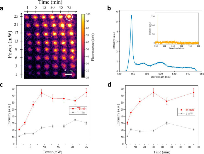
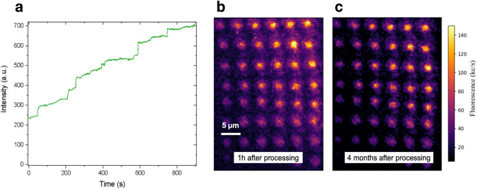
Split-vacancy color centers in diamonds are promising solid-state platforms for the implementation of photonic quantum technologies. These luminescent defects are commonly fabricated upon low-energy ion implantation and subsequent thermal annealing. Their technological uptake will require the availability of reliable methods for the controlled, large-scale production of localized individual photon emitters. This task is partially achieved by controlled ion implantation to introduce selected impurities in the host material and requires the development of challenging beam focusing or collimation procedures coupled with single-ion detection techniques. We report on the protocol for the direct optical activation of split-vacancy color centers in diamond via localized processing with a continuous-wave laser at mW optical powers. We demonstrate the activation of photoluminescent Mg- and Sn-related centers at both the ensemble and single-photon emitter levels in ion-implanted, high-purity diamond crystals without further thermal processing. The proposed lithographic method enables the activation of individual color centers at specific positions of a large-area sample by means of a relatively inexpensive equipment offering real-time, in situ monitoring of the process.

Keywords: color centers; diamond; ion implantation; laser activation; single-photon; split-vacancy.


Figures

1
1
(a) PL map of the array of spots activated in MgH-implanted diamond upon 405 nm laser processing at varying conditions of optical power and exposure time. (b) Emission spectrum, background-subtracted, and normalized to first-order Raman peak, of the spot circled in white in (a) processed for 75 min at a 25 mW optical power. The inset (orange) displays the PL spectrum acquired from a region of the sample implanted with MgH ions that did not undergo laser processing. (c) Emission intensity of the MgV ZPL as a function of the laser processing optical power for exposure times of 1 min (gray) and 75 min (red). (d) Emission intensity of the MgV ZPL as a function of the laser processing time under 1 mW (gray) and 25 mW (red) optical powers.
2
2
(a) PL map of the array of spots activated in Sn-implanted diamond upon 405 nm laser processing at varying conditions of optical power and exposure time. (b) Emission spectrum, background-subtracted, and normalized to the first-order Raman peak, of the spot circled in white in (a) processed for 75 min at a 25 mW optical power. The inset (orange) displays the PL spectrum acquired from a region of sample implanted with Sn ions which did not undergo laser processing. (c) Emission intensity of the 595 nm ZPL as a function of the laser processing optical power for exposure times of 1 min (gray) and 75 min (red). (d) Emission intensity of the 595 nm ZPL as a function of the laser processing time under 2.5 mW (gray) and 25 mW (red) optical powers.
3
3
Photoactivation dependence on the laser processing parameters for the MgV color center. The first row shows the confocal maps acquired on an array of spots undergone photoactivation via laser processing at (a) 522 nm, (b) 445 nm, and (c) 405 nm. The second row shows the integrated PL intensity (integral of the MgV ZPL spectral peak) collected spots as a function of the energy deposited on each spot under processing wavelengths of (d) 522 nm, (e) 445 nm, and (f) 405 nm. (g) Schematic representation of the energy levels of the MgV defect charge states. The negative charge state MgV is represented as a 2-level system in the diamond energy gap. Only the ground state of the doubly negative charge state MgV2– is only under the assumption that any excited state lies above the bottom of the conduction band. The colored green arrows represent the transitions induced by the processing laser at 522 nm. The shaded blue area in the gap depicts the Fermi energy range of stability of the MgV configuration, according to ref . (h) Photoassisted transitions induced by 405 and 445 nm laser processing, involving the neutral charge state of the MgV defect.
4
4
(a) Real-time MgV PL intensity under laser processing at 522 nm wavelength (5.3 mW optical power). (b, c) Confocal PL microscopy scans of the region processed with 405 nm laser. The maps were acquired under 522 nm laser excitation (100 μW optical power) (b) 1 h and (c) 4 months after the laser processing.
5
5
(a) PL map of a confocal spot in Mg-implanted diamond processed under 445 nm laser wavelength (5 mW) for 10 h, surrounded by process-induced diffraction-limited PL emitting features. (b) PL emission spectrum and second-order autocorrelation function acquired from the spot circled in white in (a). (c) MgV ZPL intensity and formation efficiency of the MgV center as a function of the laser processing wavelength and deposited energy. The tinted areas describe the 95% confidence bands.
6
6
Photoactivation dependence on the laser processing parameters for the Sn-related 595 nm color center. The first row shows the confocal maps acquired on an array of spots undergone photoactivation via laser processing at (a) 522 nm, (b) 445 nm, and (c) 405 nm. The second row shows the integrated PL intensity (integral of the 595 nm ZPL spectral peak) collected spots as a function of the energy deposited on each spot under processing wavelengths of (d) 522 nm, (e) 445 nm, and (f) 405 nm. (g) Spectrum acquired from a spot processed under a 405 nm laser at 30 J delivered energy.
7
7
(a) PL map of a confocal spot in Sn-implanted diamond processed under 445 nm laser wavelength (5 mW) for 10 h, surrounded by process-induced diffraction-limited PL emitting features. (b) PL emission spectrum and second-order autocorrelation function acquired from the spot circled in white in (a). (c) 595 nm spectrum intensity and formation efficiency of the 595 nm center as a function of the laser processing wavelength and deposited energy. The tinted areas describe the 95% confidence bands.

References

    1. Aharonovich I., Neu E.. Diamond nanophotonics. Adv. Opt Mater. 2014;2(10):911–928. doi: 10.1002/adom.201400189. - DOI
    1. Ruf M., Wan N. H., Choi H., Englund D., Hanson R.. Quantum networks based on color centers in diamond. J. Appl. Phys. 2021;130(7):070901. doi: 10.1063/5.0056534. - DOI
    1. Schröder T., Mouradian S. L., Zheng J.. et al. Quantum nanophotonics in diamond [Invited] J. Opt. Soc. Am. B. 2016;33(4):B65–B83. doi: 10.1364/JOSAB.33.000B65. - DOI
    1. Bradac C., Gao W., Forneris J., Trusheim M. E., Aharonovich I.. Quantum nanophotonics with group IV defects in diamond. Nat. Commun. 2019;10(1):5625. doi: 10.1038/s41467-019-13332-w. - DOI - PMC - PubMed
    1. Gao W. B., Imamoglu A., Bernien H., Hanson R.. Coherent manipulation, measurement and entanglement of individual solid-state spins using optical fields. Nat. Photonics. 2015;9(6):363–373. doi: 10.1038/nphoton.2015.58. - DOI

LinkOut - more resources