Review
. 2025 Jul 24;14(1):250.
doi: 10.1038/s41377-025-01923-w.

Advancements and challenges in inverse lithography technology: a review of artificial intelligence-based approaches

Affiliations
Review

Advancements and challenges in inverse lithography technology: a review of artificial intelligence-based approaches

Yixin Yang et al. Light Sci Appl. .

Abstract

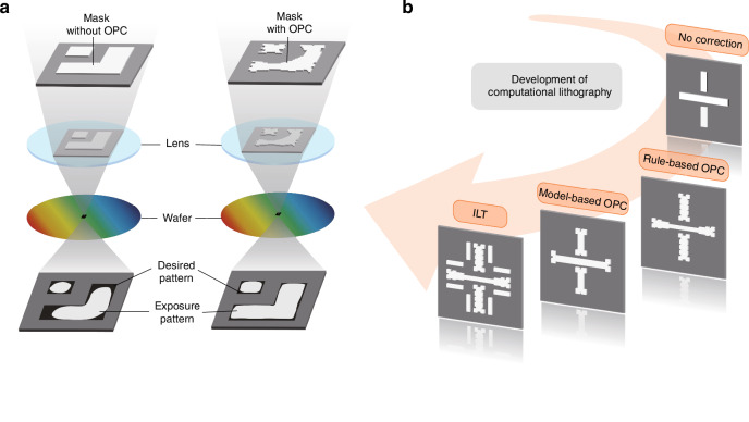
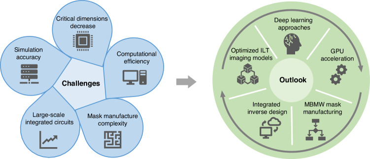
Inverse lithography technology (ILT) is a promising approach in computational lithography to address the challenges posed by shrinking semiconductor device dimensions. The ILT leverages optimization algorithms to generate mask patterns, outperforming traditional optical proximity correction methods. This review provides an overview of ILT's principles, evolution, and applications, with an emphasis on integration with artificial intelligence (AI) techniques. The review tracks recent advancements of ILT in model improvement and algorithmic efficiency. Challenges such as extended computational runtimes and mask-writing complexities are summarized, with potential solutions discussed. Despite these challenges, AI-driven methods, such as convolutional neural networks, deep neural networks, generative adversarial networks, and model-driven deep learning methods, are transforming ILT. AI-based approaches offer promising pathways to overcome existing limitations and support the adoption in high-volume manufacturing. Future research directions are explored to exploit ILT's potential and drive progress in the semiconductor industry.


Conflict of interest statement

Conflict of interest: The authors declare no competing interests.

Figures

Fig. 1
Fig. 1. Schematic of the lithography process flow in IC manufacturing and the projection lithography system.
a Principle of the lithography process in IC manufacturing. b Projection exposure system for photolithography
Fig. 2
Fig. 2. Forward imaging process of lithography and inverse process of computational lithography.
In the forward imaging process, the optical system and mask determine the wafer patterns. In computational lithography, the optimal illumination source and mask are computed based on the desired target wafer pattern
Fig. 3
Fig. 3. OPC in lithography and the evolution of computational lithography techniques.
a OPE and OPC of optical lithography. The dark shape represents the desired pattern on the wafer, and the light shape represents the exposure pattern. Distortions of OPE include unequal line widths, line end shortening, and corner rounding. OPC makes pre-distortions on masks to reduce the distortions of exposure patterns, serving as a correction for OPE. The left side shows the exposure result of the mask without OPC, and the right side presents the exposure result of the mask with OPC. b The development of computational lithography includes RBOPC, MBOPC, and ILT
Fig. 4
Fig. 4
The development history and selected milestones of ILT
Fig. 5
Fig. 5. Mask optimization using level-set method and ILT workflow.
a Level-set method for representing the mask optimization process. b The optimization procedure of ILT, including intersecting with the zero level-set for mask contour, rasterizing, computing the aerial image, calculating cost function and gradient, and optimizing gradient descent until getting the optimal mask pattern
Fig. 6
Fig. 6. The ILT mask optimization simulation under different illumination sources.
ae show the illumination sources used in computational lithography, including conventional, annular, dipole (horizontal), dipole (vertical), and quasar. ae show the initial resist patterns, the optimized masks, and the optimized resist patterns. f shows the convergence of the cost function with iteration number of ae
Fig. 7
Fig. 7. AI for computational lithography modeling, including lithography model, mask model, photoresist model, and etching model. Adapted with permission.
Copyright 2013, Society of Photo-Optical Instrumentation Engineers (SPIE). Adapted with permission. Copyright 2019, Optical Society of America. Adapted with permission. Copyright 2022, Optica Publishing Group. Adapted with permission. Copyright 2022, Optica Publishing Group. Adapted with permission. Copyright 2024, Institute of Optics and Electronics, Chinese Academy of Sciences
Fig. 8
Fig. 8. AI-based methods for lithography optimization.
a Learning-based source optimization method under the compressive sensing framework for EUV lithography. The transformation of the imaging model demonstrates the correlation between source pattern and aerial image. The simulation results obtained by the learning-based source optimization method are shown. Reproduced with permission. Copyright 2019, Optical Society of America. b EUV lithography aerial image model based on an AFCN for thick-mask effects and oblique incidence. The aerial images of test masks generated by conventional and quasar sources are presented. Adapted with permission. Copyright 2022, Optica Publishing Group. c Thick-mask model based on the DTM for thick-mask diffraction simulation by learning local DNF characteristics. The diffraction model, the real part and the imaginary components of the diffraction matrices are shown. Reproduced with permission. Copyright 2022, Optica Publishing Group. d Learning-based thick-mask model for thick-mask DNF simulation in immersion lithography. The figure demonstrates the relationship between vectorized DNF and mask, the decomposition process, and the amplitudes of diffraction matrices under oblique illumination. Adapted with permission. Copyright 2023, Optica Publishing Group. e Source-mask co-optimization method for high-NA EUV lithography. The SMO process flow, the target patterns and the optimized masks are shown. Adapted with permission. Copyright 2024, Institute of Optics and Electronics, Chinese Academy of Sciences
Fig. 9
Fig. 9. AI implementations for computational lithography and inverse lithography algorithms.
a Inverse lithography-guided GAN-OPC for mask optimization. Based on conventional GAN, the GAN-OPC improves by employing an auto-encoder structure composed of an encoder and a decoder. b Optimization results of PGAN-OPC and ILT, with each column representing a test pattern. From top to bottom, the rows display optimized masks of ILT, optimized masks of PGAN-OPC, wafer patterns of ILT, wafer patterns of PGAN-OPC, and target patterns. Reproduced with permission. Copyright 2018, Association for Computing Machinery (ACM). c VAE-based inverse layout design method
Fig. 10
Fig. 10. Model-driven deep learning methods for lithography optimization.
a Physical and mathematical representation of the lithography system. Light from the source passes through the mask, forming an image on the wafer surface. After photoresist development and etching, the printed pattern emerges. Adapted with permission. Copyright 2020, Optical Society of America. b Structure of MDL-based computational lithography and ILT methods. For coherent lithography, the MCNN framework is designed by unfolding and truncating the gradient-based ILT (SD-ILT) algorithm. The DMDL introduces parallel channels to simultaneously predict MFs and SRAFs. The PCI-MIDL employs a dual-channel architecture to accommodate the lithography system with PCI. ce demonstrate the optimized masks, printed images, and pattern errors of MCNN, DMDL and PCI-MIDL approaches. Adapted with permission. Copyright 2018, Optical Society of America. Reproduced with permission. Copyright 2020, Optical Society of America. Adapted with permission. Copyright 2020, Optical Society of America
Fig. 11
Fig. 11
Challenges and outlook of ILT. The challenges include the critical dimensions decrease, simulation accuracy, computational efficiency, large-scale integrated circuits, and mask manufacturing complexity. The outlook includes using deep learning approaches, developing optimized ILT imaging models, employing GPU acceleration, utilizing integrated inverse design, and investigating advanced mask manufacturing approaches such as MBMW

Similar articles

References

    1. Lukashchuk, A. et al. Photonic-electronic integrated circuit-based coherent LiDAR engine. Nat. Commun.15, 3134 (2024). - PMC - PubMed
    1. Li, X. K. et al. High-efficiency reinforcement learning with hybrid architecture photonic integrated circuit. Nat. Commun.15, 1044 (2024). - PMC - PubMed
    1. Wang, Y. B. et al. Photonic-circuit-integrated titanium: sapphire laser. Nat. Photonics17, 338–345 (2023).
    1. El Helou, C. et al. Mechanical integrated circuit materials. Nature608, 699–703 (2022). - PubMed
    1. Yang, Y. X. et al. A non-printed integrated-circuit textile for wireless theranostics. Nat. Commun.12, 4876 (2021). - PMC - PubMed

LinkOut - more resources