. 2025 Jul 29;16(1):6849.
doi: 10.1038/s41467-025-61886-9.

An on-chip phased array for non-classical light

Affiliations

An on-chip phased array for non-classical light

Volkan Gurses et al. Nat Commun. .

Abstract

Quantum science and technology can offer fundamental enhancements in sensing, communications and computing. The expansion from wired to wireless links is an exciting prospect for quantum technologies. For classical technologies, the advent of phased arrays enabled directional and adaptive wireless links by manipulating electromagnetic waves over free space. Here we demonstrate a phased array system on a chip that can receive, image and manipulate non-classical light over free space. We use an integrated photonic-electronic system with more than 1000 functional components on-chip to detect squeezed light. By integrating an array of 32 sub-wavelength engineered metamaterial antennas, we demonstrate a direct free-space-to-chip interface for reconfigurable quantum links. On the same chip, we implement a large-scale array of quantum-limited coherent receivers that can resolve non-classical signals simultaneously across 32 channels. With coherent readout and manipulation of these signals, we demonstrate 32-pixel imaging and spatially configurable reception of squeezed light over free space. Our work advances wireless quantum technologies that could enable practical applications in quantum communications and sensing.


Conflict of interest statement

Competing interests: V.G., S.I.D., A.H. and M.S. have filed a patent application (Quantum phased arrays, US patent application US 63/457,727; April 6, 2023). The remaining authors declare no competing interests.

Figures

Fig. 1
Fig. 1. Quantum phased arrays.
a Conceptual illustration of a wirelessly-interfaced quantum integrated circuit. b Conceptual illustration of a wireless quantum link with phased arrays. A phased array transmitter transmits a quantum state Ψ to a phased array receiver over free space. c Conceptual illustration of beamforming on squeezed light with an eight-element phased array receiver. An input field (a^in(f)) in a squeezed state is transmitted to a phased array receiver over free space. The field incident to the aperture (a^in(ρ)) is spread out over the aperture with a uniform phasefront, resulting in high geometric loss per pixel mode. After applying a phase (ϕj) and amplitude weight (gj) to each pixel mode (a^Ej), the pixel modes are combined to recover the original squeezed state. Squeezed states are represented by their Wigner functions in phase space, where Q and P represent the field quadratures (see inset).
Fig. 2
Fig. 2. Photonic-electronic system.
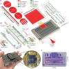
a Diagram of the photonic integrated circuit (PIC) illustrating the key building blocks, including i) the metamaterial antenna (MMA) and ii) the quantum(-limited) coherent receiver (QRX). An array of 32 MMAs couple non-classical light from free space to on-chip waveguides, followed by an array of 32 QRXs that measure the light via homodyne detection. An array of 32 thermo-optic phase shifters (TOPS) applies a phase shift to the local oscillator at each QRX. b Image of our PIC packaged with co-designed electronics, demonstrating the compact form factor of the system. The PIC is wirebonded to an interposer, which is plugged into a radio-frequency motherboard that hosts a 32-channel TIA array and the CMRR auto-correction circuit. c Die photo of the PIC showing a footprint of 3 mm  × 1.8 mm.
Fig. 3
Fig. 3. System characterization.
a Simulated far-field radiation pattern of the antenna. The radiation pattern has no grating lobes, namely scattering to higher diffraction orders, showing that the MMA is sub-wavelength engineered for diffraction-limited performance. b Noise powers of a single-channel QRX in the 32-channel system integrated over its 3-dB bandwidth for different LO powers, characterizing the shot noise clearance and LO power knee. A linear regression fit is applied to the data above the LO power knee to obtain a near-unity gradient of 1.004 ± 0.006, showing that the QRX noise floor is limited by the signal shot noise. c Output noise spectra of a single QRX for different LO powers ranging from 0 to 13.4 mW, characterizing the shot-noise-limited bandwidth. d Squeezed light detection with a single QRX using a high-speed TIA, showing squeezing and antisqueezing measured up to 5 GHz with a shot-noise-limited bandwidth of 3.70 GHz. e Shot noise clearance distribution across all channels measured with 1.54 mW LO power at each channel.
Fig. 4
Fig. 4. Squeezed light imaging.
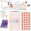
a Experimental setup for the squeezed light measurements. Squeezed light is generated off-chip and transmitted over free space to the chip (blue, Photonics), which is interfaced with electronics (orange, Electronics) for processing. b Illustration of squeezed light transmitted to the chip, showing the Wigner function of the generated squeezed vacuum state as a function of the quadrature observables (QP) and the experimental squeezing parameter (r = 1.95). c Sample means and variances of the channel output voltages as a function of time. For each channel, the sample variances are normalized to the mean variance. d Wigner functions of the 32 pixel modes characterized simultaneously as a function of the squeezing parameter (r = 1.95), phase, and geometric efficiency for each channel. The dark and light blue contours correspond to the half-maximum points of the squeezed vacuum and vacuum states, respectively.
Fig. 5
Fig. 5. Free-space quantum links.
a Conceptual illustration of beamforming on squeezed light with the chip, where a^in represents the input field and Q^out is the quadrature proportional to the combined output signal at RF. b Squeezing and antisqueezing levels as a function of the number of combined channels relative to the vacuum level after the chip is beamformed toward the squeezed light transmitter. c Squeezed light source characterization showing squeezing and antisqueezing levels as a function of source pump power for 32 combined channels. d Demonstration of reconfigurable free-space quantum links, illustrating the lack of squeezed light signal when the receiver is beamformed toward empty space (blue) and the reception of the signal when the receiver is beamformed toward the transmitter (orange). The gray trace is the vacuum signal. e Squeezing and antisqueezing levels characterizing the beamwidth of the link for 8 and 32 combined channels. f Squeezing and antisqueezing levels characterizing the field of view of the receiver for 8 and 32 combined channels. In (b, c, e, f), the orange and blue solid lines are fits of the data to a model obtained from the classical characterization of the corresponding measurement.

References

    1. Ladd, T. D. et al. Quantum computers. Nature464, 45–53 (2010). - PubMed
    1. Wehner, S., Elkouss, D. & Hanson, R. Quantum internet: a vision for the road ahead. Science362, eaam9288 (2018). - PubMed
    1. Degen, C. L., Reinhard, F. & Cappellaro, P. Quantum sensing. Rev. Mod. Phys.89, 035002 (2017).
    1. Pelucchi, E. et al. The potential and global outlook of integrated photonics for quantum technologies. Nat. Rev. Phys.4, 194–208 (2022).
    1. Wang, J., Sciarrino, F., Laing, A. & Thompson, M. G. Integrated photonic quantum technologies. Nat. Photonics14, 273–284 (2020).

LinkOut - more resources