

Low Phase Noise, Dual-Frequency Pierce MEMS Oscillators with Direct Print Additively Manufactured Amplifier Circuits
- PMID: 40731663
- PMCID: PMC12299522
- DOI: 10.3390/mi16070755
Low Phase Noise, Dual-Frequency Pierce MEMS Oscillators with Direct Print Additively Manufactured Amplifier Circuits
Abstract
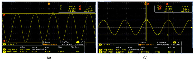
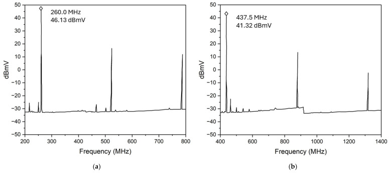
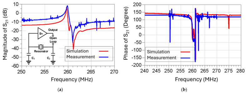
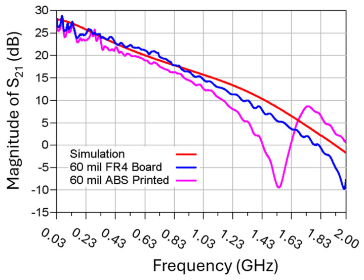
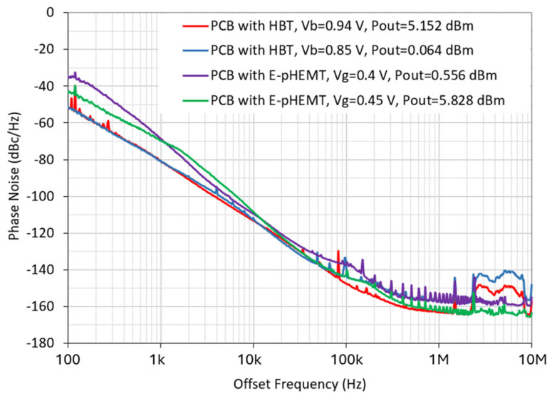
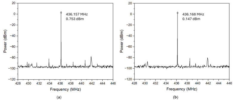
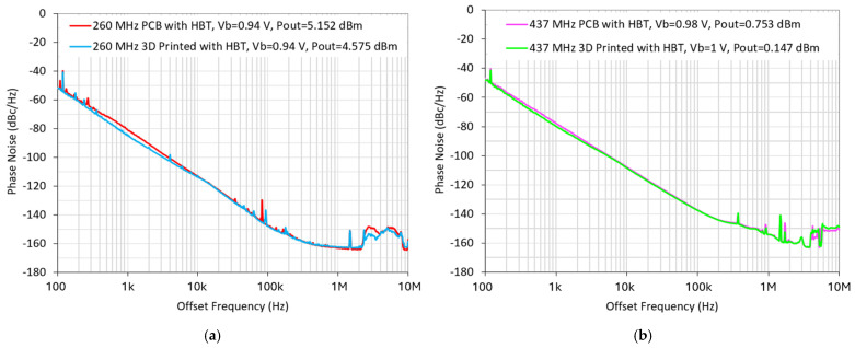
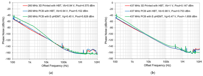
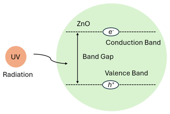
This paper presents the first demonstration and comparison of two identical oscillator circuits employing piezoelectric zinc oxide (ZnO) microelectromechanical systems (MEMS) resonators, implemented on conventional printed-circuit-board (PCB) and three-dimensional (3D)-printed acrylonitrile butadiene styrene (ABS) substrates. Both oscillators operate simultaneously at dual frequencies (260 MHz and 437 MHz) without the need for additional circuitry. The MEMS resonators, fabricated on silicon-on-insulator (SOI) wafers, exhibit high-quality factors (Q), ensuring superior phase noise performance. Experimental results indicate that the oscillator packaged using 3D-printed chip-carrier assembly achieves a 2-3 dB improvement in phase noise compared to the PCB-based oscillator, attributed to the ABS substrate's lower dielectric loss and reduced parasitic effects at radio frequency (RF). Specifically, phase noise values between -84 and -77 dBc/Hz at 1 kHz offset and a noise floor of -163 dBc/Hz at far-from-carrier offset were achieved. Additionally, the 3D-printed ABS-based oscillator delivers notably higher output power (4.575 dBm at 260 MHz and 0.147 dBm at 437 MHz). To facilitate modular characterization, advanced packaging techniques leveraging precise 3D-printed encapsulation with sub-100 μm lateral interconnects were employed. These ensured robust packaging integrity without compromising oscillator performance. Furthermore, a comparison between two transistor technologies-a silicon germanium (SiGe) heterojunction bipolar transistor (HBT) and an enhancement-mode pseudomorphic high-electron-mobility transistor (E-pHEMT)-demonstrated that SiGe HBT transistors provide superior phase noise characteristics at close-to-carrier offset frequencies, with a significant 11 dB improvement observed at 1 kHz offset. These results highlight the promising potential of 3D-printed chip-carrier packaging techniques in high-performance MEMS oscillator applications.
Keywords: MEMS; additive manufacturing; advanced packaging; oscillator; phase noise; piezoelectric; quality factor; resonators; silicon-on-insulator (SOI); zinc oxide (ZnO).
Conflict of interest statement
Author Di Lan was employed by the company Coherence. Inc.; Author Xu Han was employed by the company Qorvo, Inc; Author Tinghung Liu was employed by the company Skyworks Solutions, Inc. The remaining authors declare that the research was conducted in the absence of any commercial or financial relationships that could be construed as a potential conflict of interest.
Figures


Similar articles
-
A Novel Design of a Portable Birdcage via Meander Line Antenna (MLA) to Lower Beta Amyloid (Aβ) in Alzheimer's Disease.IEEE J Transl Eng Health Med. 2025 Apr 10;13:158-173. doi: 10.1109/JTEHM.2025.3559693. eCollection 2025. IEEE J Transl Eng Health Med. 2025. PMID: 40657533 Free PMC article.
-
Low-noise high-power dual-frequency MOPA laser with an NPRO seed.Opt Express. 2025 Feb 10;33(3):4889-4901. doi: 10.1364/OE.551172. Opt Express. 2025. PMID: 40797794
-
Low-Power MEMS-Based Pierce Oscillator Using a 61-MHz Capacitive-Gap Disk Resonator.IEEE Trans Ultrason Ferroelectr Freq Control. 2020 Jul;67(7):1377-1391. doi: 10.1109/TUFFC.2020.2969530. Epub 2020 Jan 27. IEEE Trans Ultrason Ferroelectr Freq Control. 2020. PMID: 31995483
-
Interventions to prevent occupational noise-induced hearing loss.Cochrane Database Syst Rev. 2017 Jul 7;7(7):CD006396. doi: 10.1002/14651858.CD006396.pub4. Cochrane Database Syst Rev. 2017. PMID: 28685503 Free PMC article.
-
Systemic pharmacological treatments for chronic plaque psoriasis: a network meta-analysis.Cochrane Database Syst Rev. 2017 Dec 22;12(12):CD011535. doi: 10.1002/14651858.CD011535.pub2. Cochrane Database Syst Rev. 2017. Update in: Cochrane Database Syst Rev. 2020 Jan 9;1:CD011535. doi: 10.1002/14651858.CD011535.pub3. PMID: 29271481 Free PMC article. Updated.
References
-
- Wu G., Xu J., Ng E.J., Chen W. MEMS Resonators for Frequency Reference and Timing Applications. J. Microelectromech. Syst. 2020;29:1137–1166. doi: 10.1109/JMEMS.2020.3020787. - DOI
-
- Lam C.S. A review of the recent development of MEMS and crystal oscillators and their impacts on the frequency control products industry; Proceedings of the IEEE International Ultrasonics Symposium (IUS); Beijing, China. 2–5 November 2008.
-
- Lavasani H.M., Abdolvand R., Ayazi F. A 500MHz Low Phase-Noise AlN-on-Silicon Reference Oscillator; Proceedings of the IEEE Custom Integrated Circuits Conference; San Jose, CA, USA. 16–19 September 2007.
Grants and funding
LinkOut - more resources
Full Text Sources
Miscellaneous
