. 2025 Aug 11;16(1):7385.
doi: 10.1038/s41467-025-62610-3.

Interface-controlled uniaxial in-plane ferroelectricity in Hf0.5Zr0.5O2(100) epitaxial thin films

Affiliations

Interface-controlled uniaxial in-plane ferroelectricity in Hf0.5Zr0.5O2(100) epitaxial thin films

Kai Liu et al. Nat Commun. .

Abstract

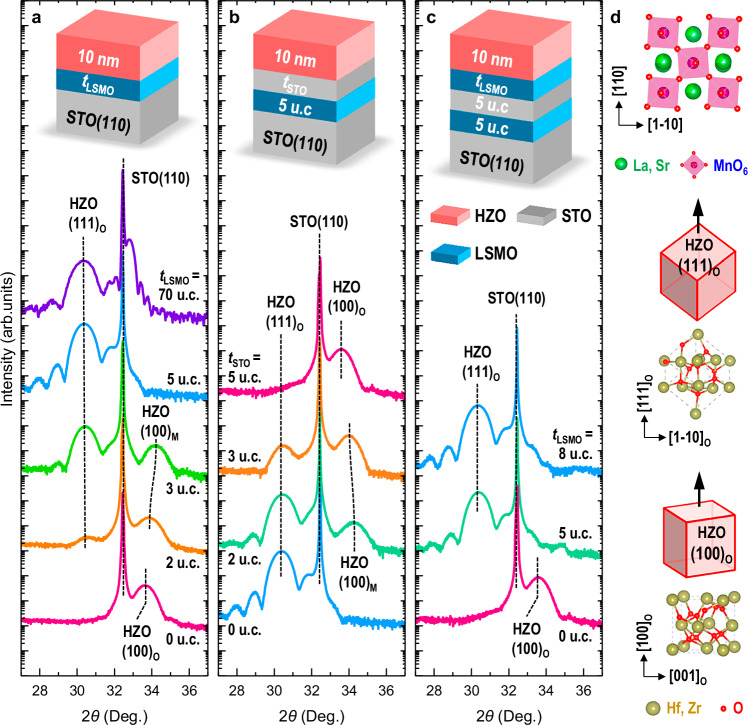
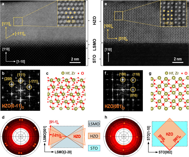
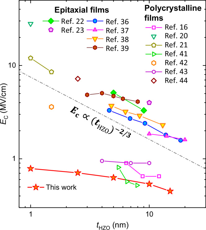
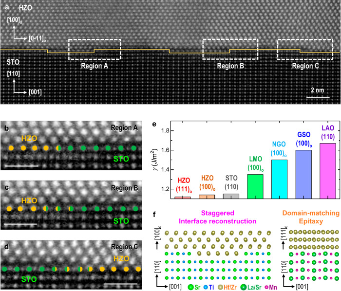
Hafnium oxide-based ferroelectric thin films are widely recognized as a CMOS-compatible and highly scalable material platform for next-generation non-volatile memory and logic devices. While out-of-plane ferroelectricity in hafnium oxide films has been intensively investigated and utilized in devices, purely in-plane ferroelectricity of hafnium oxides remains unexplored. In this work, we demonstrate a reversible structural modulation of the orthorhombic phase Hf0.5Zr0.5O2 films between (111)-oriented [HZO(111)O] multi-domain and (100)-oriented [HZO(100)O] single-domain configurations by altering perovskite oxide buffer layers. Unlike conventional out-of-plane polarized HZO(111)O films, the HZO(100)O films exhibit uniaxial in-plane ferroelectric polarization, sustained even at a thickness of 1.0 nm. Furthermore, the in-plane ferroelectric switching achieves an ultralow coercivity of ~0.5 MV/cm. The HZO(100)O phase is stabilized by a staggered interfacial reconstruction, driven by the delicate interplays between symmetry mismatch and surface energy. These findings pave the way for innovative device designs and strategies for modulating the functionalities of hafnium oxide-based ferroelectrics.


Conflict of interest statement

Competing interests: The authors declare no competing interests.

Figures

Fig. 1
Fig. 1. Structural evolutions of HZO-based heterostructures on STO(110) substrate.
a XRD 2θω linear scans of HZO films grown on LSMO-buffered STO(110) substrates. The thickness of LSMO buffer layer tLSMO varies from 0 to 70 u.c. b XRD 2θω linear scans of HZO films grown on STO/LSMO bilayer buffered STO(110) substrates. The thickness of STO layer (tSTO) varies from 0 to 5 u.c. c XRD 2θω linear scans of HZO films grown on LSMO/STO(5 u.c.)/LSMO(5 u.c.) tri-layer buffered STO(110) substrates. The thickness of the top LSMO buffer layer (tLSMO) varies from 0 to 8 u.c. The (111), (100) diffractions of orthorhombic HZO [HZO(111)O and HZO(100)O] and the (100) diffractions of monoclinic are marked by dashed lines. The insets are schematic stacking sequences of these HZO-based heterostructures. The thickness of HZO layer (tHZO) is fixed at 10 nm. d Schematic illustration of the atomic structure and growth orientations of the LSMO and orthorhombic HZO unit cell.
Fig. 2
Fig. 2. Atomic structures, domain configurations, and epitaxial relationships of HZO-based heterostructures.
a HAADF-STEM image of the HZO(10 nm)/LSMO(5 u.c.)/STO(110) heterostructure, viewed along the STO[001]c zone-axis. The inset of (a) is a zoom-in STEM image acquired from the area marked in the yellow box. b FFT pattern of a (111)O-oriented O-phase HZO domain. c Structure model of the O-phase HZO, viewed along [0-11] axis. d Left panel: Pole figure measured from the HZO(10 nm)/LSMO(5 u.c.)/STO(110) sample at 2θ ~ 30.2°. The φ and χ scanning ranges are 0–360° and 35–80°, respectively. Right panel: Schematic in-plane epitaxial relationships between the HZO(111)O domains and the underlying LSMO(110) bottom electrode. e HAADF-STEM image of the HZO(10 nm)/STO(110) heterostructure, viewed along the HZO[001]O axis. The inset displays a zoom-in image acquired from the area marked in the yellow box. f FFT pattern of a (100)O-oriented O-phase HZO domain. g Structure model of the O-phase HZO, viewed along the HZO[001]O axis. h Left panel: Pole figure about {11-1} peaks measured from the HZO/STO sample at 2θ ~ 30.2°, The φ and χ ranges are 0–360° and 35–80°, respectively. Right panel: Schematic in-plane epitaxial relationships between the HZO(100)O lattice and the STO(110) substrate.
Fig. 3
Fig. 3. Ferroelectric characterizations of HZO/STO(110) films.
a Schematic diagram and optical microscopic image of the HZO(10 nm)/STO(110) film with interdigitated Pt electrodes for the in-plane FE characterizations. b, c Electric field-dependent in-plane polarization (Pin-E) hysteresis loops measured from the HZO(10 nm)/STO(110) film with E//HZO[001]O (b) and E//HZO[010]O (c). The E scanning range (Emax) varies from 0.5 to 0.9 MV/cm. d E-dependent out-of-plane polarization (Pout-E) hysteresis loops measured from the 10 nm thick HZO film grown on Nb:STO(110) substrate. The E scanning range (Emax) varies from 2.0 to 6.0 MV/cm. The inset displays the measurement geometry. The top electrodes are circular-shaped Pt pads. e Left panel: Schematic diagram of switching the in-plane FE polarization through the tip-induced trailing field. The bias applied on the PFM tip (Vtip) is ±7 V. Right panel: Schematic diagram for PFM measurements on uniaxial polarization of HZO(100)O/STO(110) sample. The angle between PFM slow-scan axis and HZO[001]O axis is defined as θscan. In-plane PFM phase (f) and amplitude (g) images with θscan = 0°, 45°, 60°, and 90°. The scanning area is 4 × 4 μm2.
Fig. 4
Fig. 4. Ultra-low coercivity of HZO(100)O/STO(110) films.
tHZO-dependent coercive fields (EC) derived from the HZO(100)O/STO(100) films with various tHZO. A series of tHZO-EC curves extracted from references are also inserted for comparison. The tHZO-EC curves of epitaxial (polycrystalline) HZO films are plotted in solid (open) symbols for clarity. The EC (tHZO)−2/3 relationship is marked by a dash-dot line.
Fig. 5
Fig. 5. Interface reconstruction in the HZO(100)O/STO(110) film.
a HAADF-STEM image measured near the HZO/STO(110) interface, viewed along STO[11¯0] zone axis. The solid line (yellow) marks the laterally staggered interface. bd Zoom-in STEM images with HZO/STO step-like atomic contrasts, acquired from 3 pre-selected regions (marked by dashed boxes in (a)). The atomic contrasts of Hf(Zr) and Sr are labeled by orange and green circles, respectively. The mixed Hf(Zr) and Sr contrasts are marked by the bi-color circles. e DFT-calculated surface energies (γ) of different HZO(111)O, HZO(100)O, and several representative pseudo-cubic (110)-oriented ABO3 surfaces. f Schematic atomic structure of HZO(100)O/STO(110) interface with staggered reconstruction and HZO(111)O/LSMO(110) interface with domain-matching epitaxy growth mode.

Similar articles

References

    1. Dawber, M., Rabe, K. M. & Scott, J. F. Physics of thin-film ferroelectric oxides. Rev. Mod. Phys.77, 1083–1130 (2005).
    1. Khan, A. I., Keshavarzi, A. & Datta, S. The future of ferroelectric field-effect transistor technology. Nat. Electron.3, 588–597 (2020).
    1. Garcia, V. & Bibes, M. Ferroelectric tunnel junctions for information storage and processing. Nat. Commun.5, 4289 (2014). - PubMed
    1. Mikolajick, T. et al. Next generation ferroelectric materials for semiconductor process integration and their applications. J. Appl. Phys.129, 100901 (2021).
    1. Chen, Z. et al. Study of strain effect on in-plane polarization in epitaxial BiFeO3 thin films using planar electrodes. Phys. Rev. B86, 235125 (2012).

LinkOut - more resources