

Growth and Characterization of Ga2O3 for Power Nanodevices Using Metal Nanoparticle Catalysts
- PMID: 40801708
- PMCID: PMC12348871
- DOI: 10.3390/nano15151169
Growth and Characterization of Ga2O3 for Power Nanodevices Using Metal Nanoparticle Catalysts
Abstract
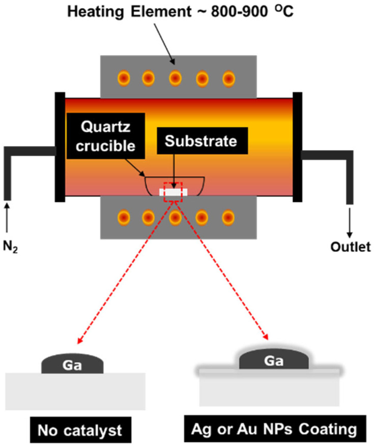
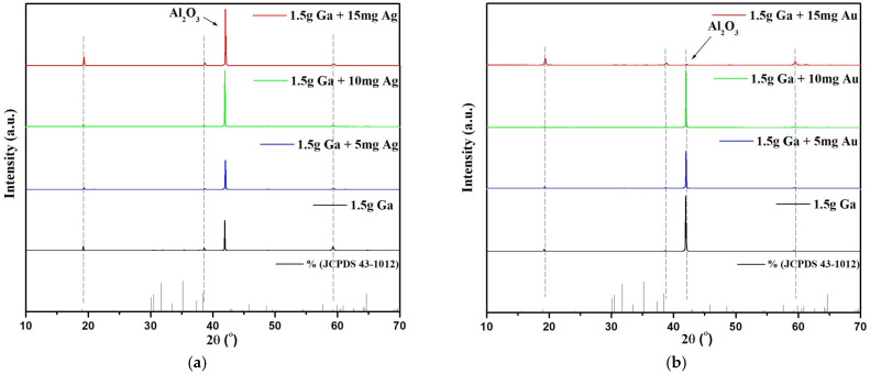
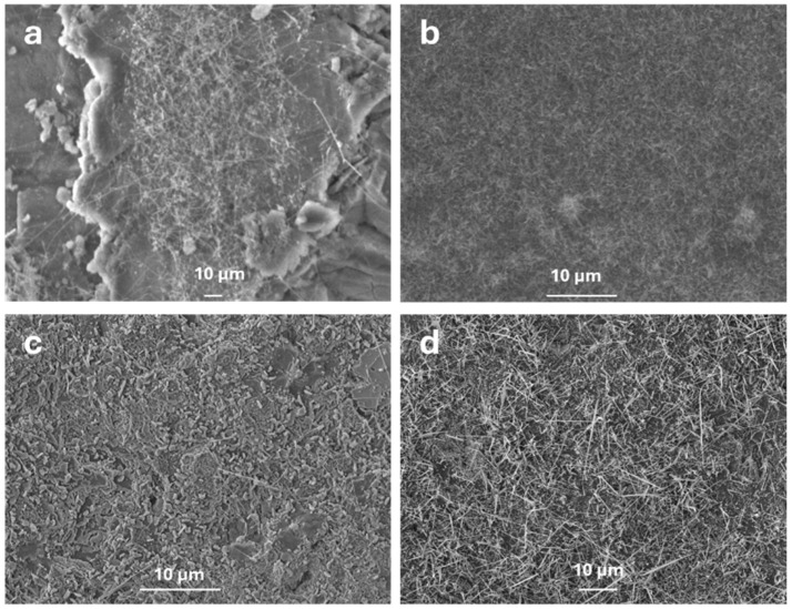
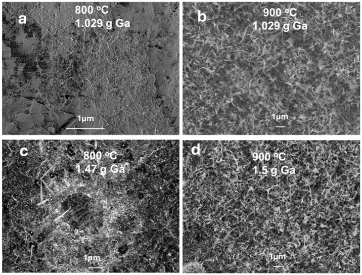
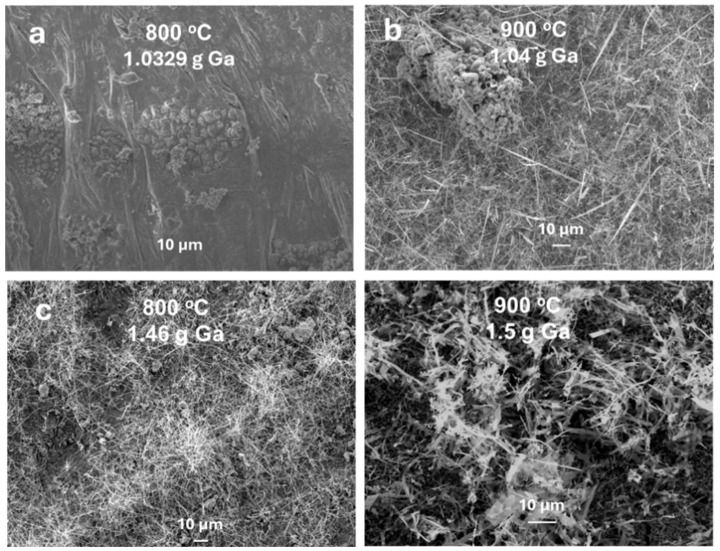
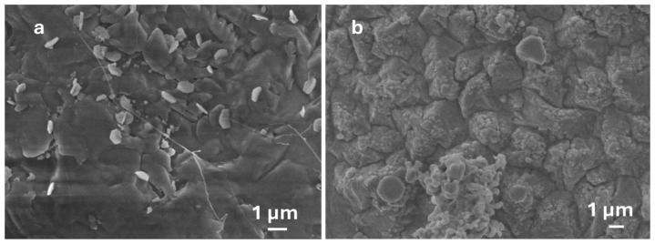
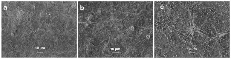
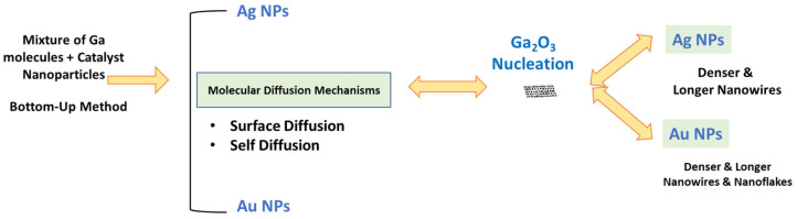
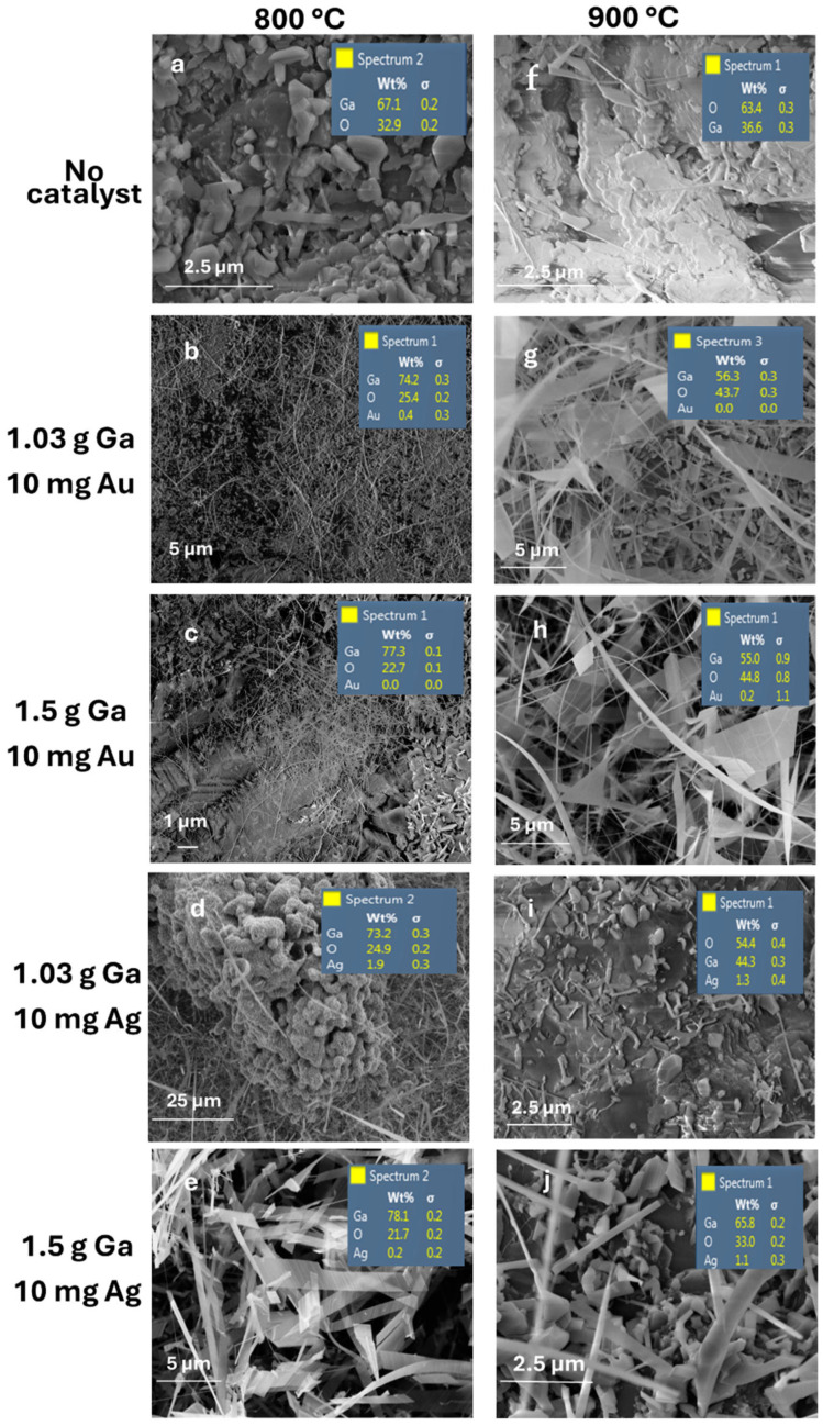
A simple and inexpensive thermal oxidation process is used to grow β-Ga2O3 oxide (β-Ga2O3) thin films/nanorods on a c-plane (0001) sapphire substrate using Ag/Au catalysts. The effect of these catalysts on the growth mechanism of Ga2O3 was studied by different characterization techniques, including X-ray diffraction analysis (XRD), Scanning Electron Microscopy (SEM), and Energy Dispersive X-ray analysis (EDX). The XRD results of the grown Ga2O3 on a sapphire substrate show three sharp diffraction peaks located at 19.31°, 38.70° and 59.38° corresponding to the 2¯01, 4¯02 and 6¯03 planes of β-Ga2O3. Field Emission Scanning Electron Microscope (FESEM) analysis showed the formation of longer and denser Ga2O3 nanowires at higher temperatures, especially in the presence of silver nanoparticles as catalysts.
Keywords: catalysts; gold; silver; thermal oxidation; β-Ga2O3.
Conflict of interest statement
The authors declare no conflicts of interest.
Figures
Similar articles
-
Opto-electronic properties of Sn-C Co-doped β-Ga2O3 at different concentrations: a GGA + U study.J Mol Model. 2025 Aug 1;31(8):224. doi: 10.1007/s00894-025-06459-9. J Mol Model. 2025. PMID: 40748471
-
Nanoplasmonic Au-Ag Alloy Coatings on the Surface of TiO2 Nanotubes for Vitamin B12 Detection by Surface-Enhanced Raman Scattering Spectroscopy.ACS Omega. 2025 Jun 12;10(24):25555-25568. doi: 10.1021/acsomega.5c01060. eCollection 2025 Jun 24. ACS Omega. 2025. PMID: 40584309 Free PMC article.
-
High-Performance Solar-Blind Photodetector Based on (010)-Plane β-Ga2O3 Thermally Oxidized from Nonpolar (110)-Plane GaN.ACS Appl Mater Interfaces. 2024 Apr 24;16(16):20794-20802. doi: 10.1021/acsami.4c01806. Epub 2024 Apr 11. ACS Appl Mater Interfaces. 2024. PMID: 38602968
-
Management of urinary stones by experts in stone disease (ESD 2025).Arch Ital Urol Androl. 2025 Jun 30;97(2):14085. doi: 10.4081/aiua.2025.14085. Epub 2025 Jun 30. Arch Ital Urol Androl. 2025. PMID: 40583613 Review.
-
Phytogenic nanoparticles: synthesis, characterization, and their roles in physiology and biochemistry of plants.Biometals. 2024 Feb;37(1):23-70. doi: 10.1007/s10534-023-00542-5. Epub 2023 Nov 2. Biometals. 2024. PMID: 37914858 Review.
References
-
- Shi Q., Wang Q., Zhang D., Wang Q., Li S., Wang W., Fan Q., Zhang J. Structural, optical and photoluminescence properties of Ga2O3 thin films deposited by vacuum thermal evaporation. J. Lumin. 2019;206:53–58. doi: 10.1016/j.jlumin.2018.10.005. - DOI
-
- Hu J., Yu B., Zhou J. New Generation Beta-Gallium Oxide Nanomaterials: Growth and Performances in Electronic Devices. Adv. Eng. Mater. 2023;25:2300688. doi: 10.1002/adem.202300688. - DOI
Grants and funding
LinkOut - more resources
Full Text Sources
