

Epitaxial Graphene/n-Si Photodiode with Ultralow Dark Current and High Responsivity
- PMID: 40801728
- PMCID: PMC12348325
- DOI: 10.3390/nano15151190
Epitaxial Graphene/n-Si Photodiode with Ultralow Dark Current and High Responsivity
Abstract
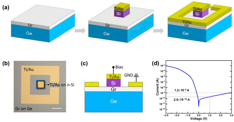
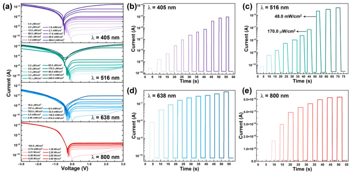
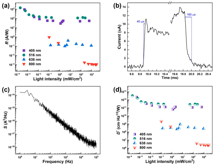
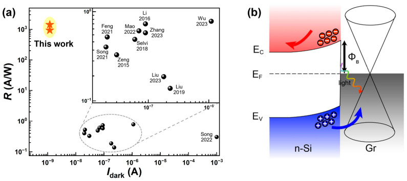
Graphene's exceptional carrier mobility and broadband absorption make it promising for ultrafast photodetection. However, its low optical absorption limits responsivity, while the absence of a bandgap results in high dark current, constraining the signal-to-noise ratio and efficiency. Although silicon (Si) photodetectors normally offer fabrication compatibility, their performance is severely hindered by interface trap states and optical shading. To overcome these limitations, we demonstrate an epitaxial graphene/n-Si heterojunction photodiode. This device utilizes graphene epitaxially grown on germanium integrated with a transferred Si thin film, eliminating polymer residues and interface defects common in transferred graphene. As a result, the fabricated photodetector achieves an ultralow dark current of 1.2 × 10⁻⁹ A, a high responsivity of 1430 A/W, and self-powered operation at room temperature. This work provides a strategy for high-sensitivity and low-power photodetection and demonstrates the practical integration potential of graphene/Si heterostructures for advanced optoelectronics.
Keywords: graphene; heterojunction; n-type silicon; photodetector; self-powered operation.
Conflict of interest statement
The authors declare no conflicts of interest.
Figures
Similar articles
-
On-chip graphene photodetectors with a nonvolatile p-i-n homojunction.Light Sci Appl. 2025 Jul 7;14(1):238. doi: 10.1038/s41377-025-01832-y. Light Sci Appl. 2025. PMID: 40623980 Free PMC article.
-
Enhancing the photoresponse performance of graphene on silicon-based heterojunction as a broadband photodetector.Sci Rep. 2025 Jul 25;15(1):27139. doi: 10.1038/s41598-025-13266-y. Sci Rep. 2025. PMID: 40715351 Free PMC article.
-
Waveguide-integrated PdSe2/MoS2 van der Waals heterojunction photodetector on a thin-film lithium niobate platform.Appl Opt. 2025 Jun 20;64(18):5115-5120. doi: 10.1364/AO.564072. Appl Opt. 2025. PMID: 40792806
-
Research Progress and Future Perspectives on Photonic and Optoelectronic Devices Based on p-Type Boron-Doped Diamond/n-Type Titanium Dioxide Heterojunctions: A Mini Review.Nanomaterials (Basel). 2025 Jun 29;15(13):1003. doi: 10.3390/nano15131003. Nanomaterials (Basel). 2025. PMID: 40648710 Free PMC article. Review.
-
Home treatment for mental health problems: a systematic review.Health Technol Assess. 2001;5(15):1-139. doi: 10.3310/hta5150. Health Technol Assess. 2001. PMID: 11532236
References
-
- Mak K.F., Ju L., Wang F., Heinz T.F. Optical Spectroscopy of Graphene: From the Far Infrared to the Ultraviolet. Solid. State Commun. 2012;152:1341–1349. doi: 10.1016/j.ssc.2012.04.064. - DOI
-
- Li Z.Q., Henriksen E.A., Jiang Z., Hao Z., Martin M.C., Kim P., Stormer H.L., Basov D.N. Dirac Charge Dynamics in Graphene by Infrared Spectroscopy. Nat. Phys. 2008;4:532–535. doi: 10.1038/nphys989. - DOI
Grants and funding
LinkOut - more resources
Full Text Sources
Research Materials
