

Current matched all perovskite tandem solar cells with low lead perovskites achieving 31.9% efficiency and enhanced stability
- PMID: 40804298
- PMCID: PMC12350632
- DOI: 10.1038/s41598-025-99575-8
Current matched all perovskite tandem solar cells with low lead perovskites achieving 31.9% efficiency and enhanced stability
Abstract
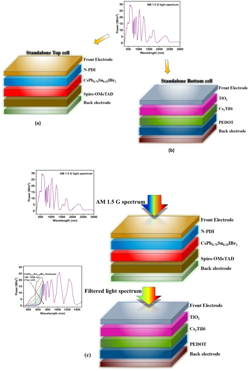
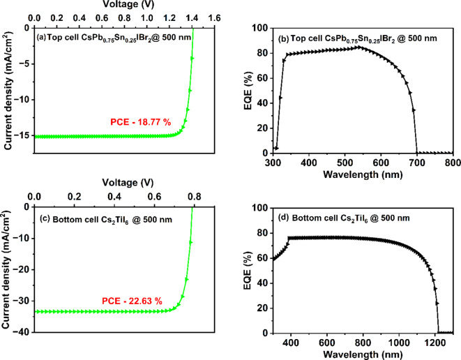
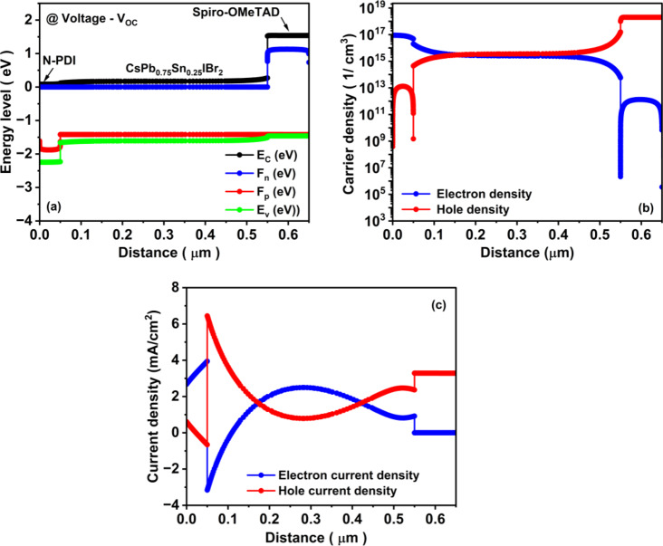
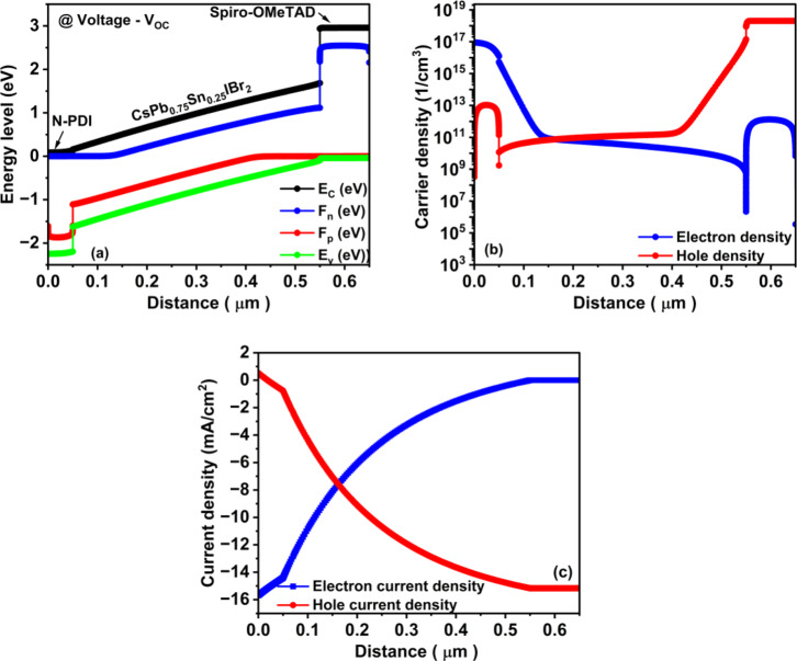
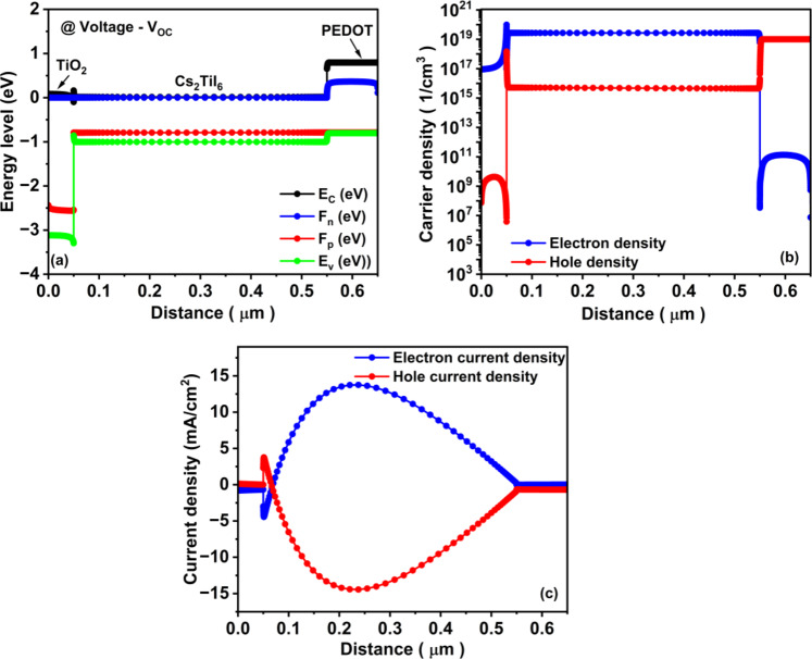
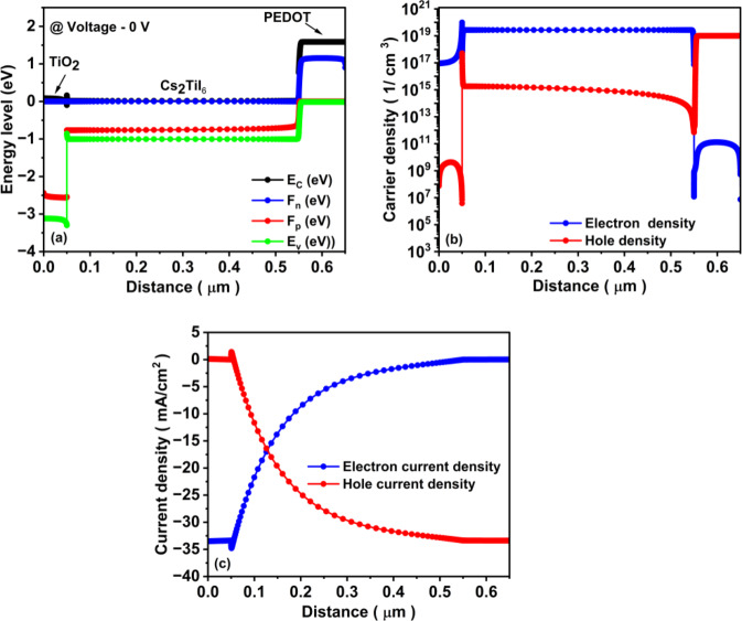
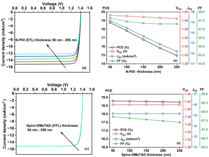
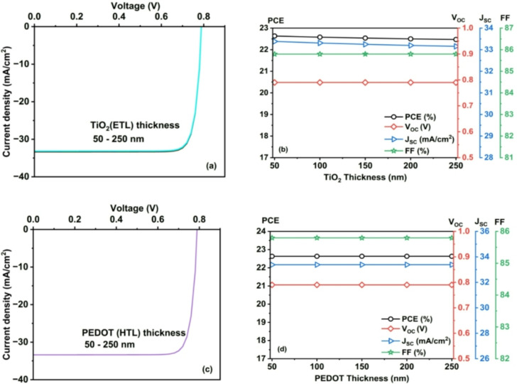
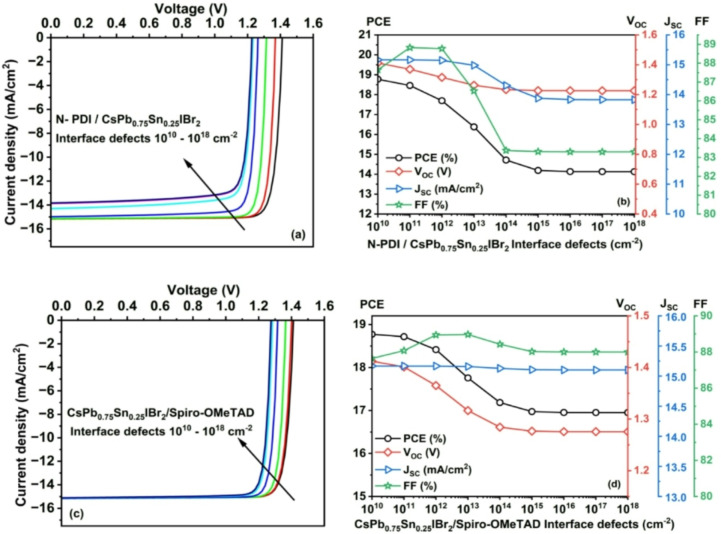
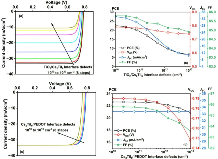
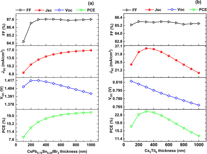
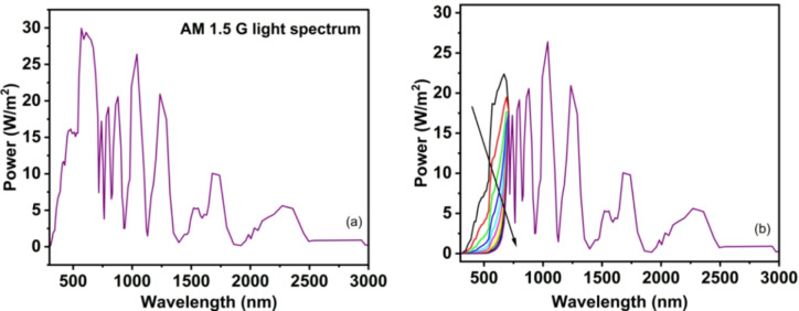
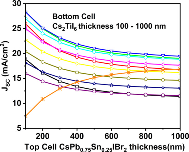
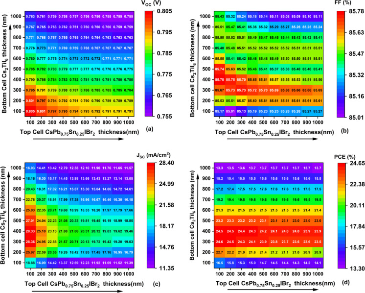
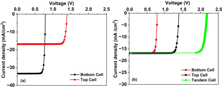
Multilayer tandem solar cells emerge as a transformative solution, leveraging multiple absorber layers with optimized bandgaps to capture and convert a broader spectrum of sunlight. This layered architecture overcomes the efficiency limitations of single-junction solar cells by minimizing transparency and thermalization losses while maximizing photon utilization across the solar spectrum. Although hybrid perovskites have demonstrated exceptional photovoltaic performance, their dependence on organic components often results in stability challenges under varying environmental conditions. To mitigate this issue, all-inorganic perovskites have emerged as a robust alternative, offering enhanced thermal and moisture stability along with reliable long-term performance. In the proposed design, a sustainable approach is adopted using a tin-based, low-lead, all-inorganic CsPb0.75Sn0.25IBr2 (1.78 eV) for the top subcell absorber, paired with a lead-free double perovskite Cs2TiI6 (1.02 eV), in the bottom subcell, with the use of SCAPS - 1D simulator. Standalone analyses of the top and bottom subcells are conducted before tandem configuration implementation. Importantly, tandem design is optimized by investigating the current matching point by varying the absorber layer thicknesses (100-1000 nm). Illuminating the top subcell with the AM 1.5G spectrum and passing filtered light to the bottom subcell enables extensive light absorption and improved overall PCE. With a common current point at 16.83 mA/cm2 the tandem design attains a peak PCE of 31.93%, accompanied by a fill factor (FF) of 86.84% and an open-circuit voltage (VOC) of 2.18 V. These findings highlight the potential of this optimized tandem solar cell design to deliver high efficiency with enhanced stability, offering a promising pathway for sustainable and scalable photovoltaic technologies.
Keywords: Double perovskite; Low - lead all inorganic perovskite; SCAPS−1D; Tandem solar cell.
© 2025. The Author(s).
Conflict of interest statement
Declarations. Competing interests: The authors declare no competing interests. Consent to participate: We comply with the ethical standards. We provide our consent to take part. Consent for publication: All the authors are giving consent to publish.
Figures
Similar articles
-
Numerical Simulation Analysis of Two-Terminal Monolithic Perovskite-CIGS Tandem Solar Cell for Enhanced Photovoltaic Performance Using SCAPS-1d.Langmuir. 2025 Aug 5;41(30):19729-19741. doi: 10.1021/acs.langmuir.5c01551. Epub 2025 Jul 23. Langmuir. 2025. PMID: 40700735
-
Prescription of Controlled Substances: Benefits and Risks.2025 Jul 6. In: StatPearls [Internet]. Treasure Island (FL): StatPearls Publishing; 2025 Jan–. 2025 Jul 6. In: StatPearls [Internet]. Treasure Island (FL): StatPearls Publishing; 2025 Jan–. PMID: 30726003 Free Books & Documents.
-
A numerical investigation to design and performance optimization of lead-free Cs2TiCl6 based perovskite solar cells with different charge transport layers.Sci Rep. 2025 Jul 1;15(1):20768. doi: 10.1038/s41598-025-06820-1. Sci Rep. 2025. PMID: 40594432 Free PMC article.
-
Monolithic Perovskite/Perovskite/Silicon Triple-Junction Solar Cells: Fundamentals, Progress, and Prospects.Nanomicro Lett. 2025 Jul 21;18(1):8. doi: 10.1007/s40820-025-01836-8. Nanomicro Lett. 2025. PMID: 40690082 Free PMC article. Review.
-
All-Inorganic Tin-Containing Perovskite Solar Cells: An Emerging Eco-Friendly Photovoltaic Technology.Adv Mater. 2025 Jul;37(29):e2505543. doi: 10.1002/adma.202505543. Epub 2025 May 12. Adv Mater. 2025. PMID: 40350985 Review.
References
-
- Wang, K. et al. Overcoming Shockley-Queisser limit using halide perovskite platform? Joule 6 (4), 756–771 (2022).
-
- Song, T. B. et al. Perovskite solar cells: film formation and properties. J. Mater. Chem. A. 3 (17), 9032–9050 (2015).
-
- Kim, J. Y., Lee, J. W., Jung, H. S., Shin, H. & Park, N. G. High-Efficiency Perovskite Solar Cells Chem. Rev.120 (15), 7867–7918 (2020). - PubMed
-
- Yang, Z., Zhang, S., Li, L. & Chen, W. Research progress on large-area perovskite thin films and solar modules. J. Materiom. 3 (4), 231–244 (2017).
-
- Habibi, M., Zabihi, F., Ahmadian-Yazdi, M. R. & Eslamian, M. Progress in emerging solution-processed thin film solar cells–Part II: perovskite solar cells. Renew. Sustain. Energy Rev.62, 1012–1031 (2016).
LinkOut - more resources
Full Text Sources
