Review
. 2025 Jun 28;5(8):2500013.
doi: 10.1002/smsc.202500013. eCollection 2025 Aug.

Recent Advances in the Synthesis, Optical Properties, and Applications of Fluorescent Silicon Carbide Quantum Dots

Affiliations
Review

Recent Advances in the Synthesis, Optical Properties, and Applications of Fluorescent Silicon Carbide Quantum Dots

Mahdi Hasanzadeh Azar et al. Small Sci. .

Abstract

Earth-abundant, fluorescent silicon carbide (SiC) quantum dots (QDs) have recently attracted remarkable attention on account of their long-term chemical and optical stability and impressive biocompatibility. However, there has been a long-standing debate among researchers concerning whether radiative recombination in SiC QDs is governed by quantum confinement effects or by surface-related states. Herein, the underlying mechanism responsible for the photoluminescence observed in SiC QDs is elucidated. Significant progress made through the development of advanced strategies for synthesizing ultrasmall SiC QDs and modifying their surfaces with functional groups, conjugated molecules, and protective shells is discussed. Subsequently, the potential for engineered SiC QDs to be applied to a range of sectors, including energy (photocatalytic-based CO2 reduction systems), electronics/optoelectronics (electroluminescent white light-emitting diodes, nonlinear optics, and quantum sensing), and biomedicine (cell imaging and biosensors), is reviewed. Finally, this review is summarized with some forward-looking challenges and prospects.

Keywords: fluorescent quantum dots; optical properties; optoelectronic and biomedical and energy applications; silicon carbide; surface modifications.


Conflict of interest statement

The authors declare no conflict of interest.

Figures

Figure 1
Figure 1
a) The primitive hexagonal unit cells and stacking sequence of 3C‐, 4H‐, and 6H‐SiC. Reproduced with permission.[ 252 ] Copyright 2013, American Chemical Society. Band structures of b) 3C, c) 4H, and d) 6H SiC. Reproduced with permission.[ 253 ] Copyright 2020, AIP Publishing.
Figure 2
Figure 2
a) Mechanism of donor–acceptor recombination. Reproduced with permission.[ 47 ] Copyright 2024, Springer Nature. b) PL spectra with N‐Al doped 6H‐SiC at a series of temperatures. Reproduced with permission.[ 49 ] Copyright 2024, DTU Orbit. c) Illustration of DAP and e‐A recombination within the band structure. Reproduced with permission.[ 14 ] Copyright 2019, IOP Publishing. d) Fitting PL spectra of co‐doped 4H‐SiC at different temperatures. Reproduced with permission.[ 48 ] Copyright 2022, Elsevier. e) Mechanism of white light emission by combining two DAPs in 4H‐SiC. Reproduced with permission.[ 51 ] Copyright 2015, IOP Publishing. f) PL spectra of B‐N doped 6H‐SiC with two boron concentrations: 1.65 × 1018 cm−3 in A1 and 4.14 × 1018 cm−3 in A2. Reproduced with permission.[ 48 ] Copyright 2022, Elsevier. g) PL spectra of B‐N doped 6H‐SiC with series of B and N concentrations (a: N A = 8.0 × 1018 cm−3 and N D = 0.04 × 1018 cm−3, b: N A = 6.9 × 1018 cm−3 and N D = 3.2 × 1018 cm−3, c: N A = 6.9 × 1018 cm−3 and N D = 6.0 × 1018 cm−3, d: N A = 4.4 × 1018 cm−3 and N D = 9.0 × 1018 cm−3, and e: N A = 5.2 × 1018 cm−3 and N D = 9.2 × 1018 cm−3). Reproduced with permission.[ 52 ] Copyright 2019, IOP Publishing.
Figure 3
Figure 3
a) PL spectra of D1 defects in SiC. b) Recombination mechanism of D1 defects. Reproduced with permission.[ 19 ] Copyright 2003, Elsevier. c) PL spectra for each center of threading dislocations. d) Band structure illustration for threading dislocations. Reproduced with permission.[ 56 ] Copyright 2022, American Chemical Society. e,f) Recombination related to threading dislocation with deep levels in low and high concentrations. Reproduced with permission.[ 57 ] Copyright 2011, AIP Publishing. g–i) PL spectra of Frenkel defects in intrinsic, extrinsic, and multiple‐layer SF in 4H‐SiC. Reproduced with permission.[ 58 ] Copyright 2010, AIP Publishing.
Figure 4
Figure 4
a) Preparation method of porous 6H‐SiC. B,c) Microstructure of porous 6H‐SiC with different pore sizes. Reproduced with permission.[ 62 ] Copyright 2013, IOP Publishing. d) Structure of 6H‐SiC with bulk substrate and porous layer, as well as the mechanism of each part of the samples within the band structure. e) PL spectra of the prepared 6H‐SiC sample with three peaks corresponding to different mechanisms. Reproduced with permission.[ 66 ] Copyright 2017, Springer Nature.
Figure 5
Figure 5
a) 3C‐SiC nanowires with nanocylinder morphology. b) PL spectra of each nanostructure. Reproduced with permission.[ 83 ] Copyright 2008, IOP Publishing. c) PL spectra of 6H‐SiC nanowires. Reproduced with permission.[ 84 ] Copyright 2008, IOP Publishing. d) Computational band structure of 2D SiC. Reproduced with permission.[ 47 ] Copyright 2024, Springer Nature.
Figure 6
Figure 6
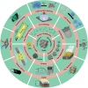
Schematic diagram of a broad spectrum of developments in synthesis, optical properties, and applications of SiC QDs.
Figure 7
Figure 7
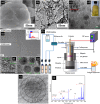
3C‐SiC powders a) before and b) after etching. c) HRTEM and d) photographs of 3C‐SiC NCs aqueous colloidal suspension. Reproduced with permission.[ 95 ] Copyright 2014, Scientific Research Publishing. e) TEM images and the size distributions of the colloidal suspensions of 3C‐SiC QDs in ethanol and water. HRTEM images of the SiC QDs in f) water and g) ethanol. Reproduced with permission.[ 103 ] Copyright 2014, AIP Publishing. h) Schematic diagram of the non‐thermal process design. Reproduced with permission.[ 115 ] Copyright 2021, American Ceramic Society. i) TEM image of a 4.4 nm carbon‐coated 3C‐SiC NC. Reproduced with permission.[ 106 ] Copyright 2015, IOP Publishing. j) Emission spectrum of arc plasma Reproduced with permission.[ 113 ] Copyright 2021, Elsevier.
Figure 8
Figure 8
a) Schematic diagram showing the synthesis process of 3C‐SiC NCs via nonthermal plasma. Reproduced with permission.[ 29 ] Copyright 2021, American Chemical Society. b,c) The effect of exposure time on the arc plasma shape. Reproduced with permission.[ 115 ] Copyright 2021, American Ceramic Society. TEM images of 3C‐SiC NCs prepared at precursor flow rates of d) 0.4 sccm, e) 2.4 sccm, and f) 5 sccm. Reproduced with permission.[ 117 ] Copyright 2016, Royal Society of Chemistry.
Figure 9
Figure 9
TGA of 3C‐SiC NCs a) baked for excess carbon removal and b) baked for silicon oxidation. Reproduced with permission.[ 120 ] Copyright 2022, American Chemical Society. c) Atomic concentrations of Si, C, and O of 3C‐SiC NCs in the presence and absence of H2. Reproduced with permission.[ 115 ] Copyright 2021, American Ceramic Society. d) The voltage and current waveforms for one discharge at 22 kV/500 ns. Reproduced with permission.[ 124 ] Copyright 2021, Springer Nature. e) Schematic diagram of electrical discharge setup for synthesis of SiC NCs. f) TEM image of 3C‐SiC NCs formed by the electrical discharge process. Reproduced with permission.[ 125 ] Copyright 2022, Springer Nature. TEM images of particles formed by discharge between g) Si—C electrodes in CHX at 22 kV/500 ns h) C—C electrodes in TMS at 22 kV/500 ns, i) SAED pattern of NPs formed by discharge between C—C electrodes in TMS at 22 kV/500 ns, and j) C—C electrodes in TMS at 8 kV/100 ns. Reproduced with permission.[ 124 ] Copyright 2021, Springer Nature.
Figure 10
Figure 10
a) Schematic diagram of molten salt electrochemical mechanism for 3C‐SiC NPs formation. b) Experimental setup for the PLA in liquid. Reproduced with permission.[ 140 ] Copyright 2022, Elsevier. c) Schematic diagram of the ablation process at the interface of 6 H‐SiC and different solvents. Reproduced with permission.[ 152 ] Copyright 2015, American Chemical Society. d) TEM image of NCs prepared by ablating the 4 H‐SiC substrate with the corresponding lattice spacing. e) XRD spectra for the SiC NCs formed by laser ablating of a 4 H‐SiC substrate with a fluence of 1.67 J cm−2. Reproduced with permission.[ 148 ] Copyright 2019, AIP Publishing. f) TEM image of NCs prepared by nanosecond laser irradiation. g) SAED pattern of the selected region. h) TEM image of NCs prepared by femtosecond laser irradiation. i) SAED pattern of the selected region. Reproduced with permission.[ 150 ] Copyright 2022, Springer Nature.
Figure 11
Figure 11
TEM images of 4H‐SiC NCs prepared under various laser fluxes of a) 5.31, b) 3.54 c) and 1.77 J cm−2. Reproduced with permission.[ 42 ] Copyright 2022, Elsevier. d) 4H‐SiC NCs colloidal suspensions prepared at different laser fluences (increase of fluence from left to right). Reproduced with permission.[ 151 ] Copyright 2018, Springer Nature. e) UV–vis spectra of SiC bulk and NCs prepared by various laser fluences. Reproduced with permission.[ 42 ] Copyright 2022, Elsevier. XRD pattern of 6H‐SiC NPs produced in f) water and g) ethanol with their corresponding SAED patterns. Reproduced with permission.[ 42 ] Copyright 2022, Elsevier. h) TEM and AFM images of 2D SiC QDs. Reproduced with permission.[ 158 ] Copyright 2018, Springer Nature. i) TEM image and SAED pattern of 3C‐SiC NCs formed by the combination of etching and hydrothermal processes. Reproduced with permission.[ 168 ] Copyright 2016, AIP Publishing.
Figure 12
Figure 12
a) PL maxima, PLE, and absorption spectra of 3C‐SiC NCs with different sizes and functional groups. b) The relation between size and excitation energy. c) Schematic diagram showing the relation between bandgap and particle size. Reproduced with permission.[ 174 ] Copyright 2018, American Chemical Society.
Figure 13
Figure 13
Energy band diagrams of bulk 3C‐SiC, experimental SiC NCs with various sizes, and theoretical calculations of H‐terminated and co‐H and partial Si═O terminated 3C‐SiC NC (1.5 nm). Reproduced with permission.[ 29 ] Copyright 2020, American Chemical Society.
Figure 14
Figure 14
a) Calculated DFT of the 3C‐SiC NC with oxygen termination on double bond sites. Reproduced with permission.[ 29 ] Copyright 2020, American Chemical Society. b) PL spectra of 3C‐SiC NCs aqueous suspension. Reproduced with permission.[ 178 ] Copyright 2015, Royal Society of Chemistry. c) PL spectra of Sample II that underwent aggregation and size enlargement. Reproduced with permission.[ 178 ] Copyright 2015, Royal Society of Chemistry. d) HOMOs of the 2 nm 3C‐SiC QDs terminated by H, OH, F. Reproduced with permission.[ 186 ] Copyright 2016, Royal Society of Chemistry. e) Illustration diagram and f) PL spectra of different surface‐terminated SiC NCs. g) Decay‐associated spectra (DAS) of as‐prepared and reduced samples. Reproduced with permission.[ 189 ] Copyright 2016, American Chemical Society.
Figure 15
Figure 15
PL a,c,e,g) and PLE b,d,f,h) spectra of (a,b) the 3C‐SiC NC aqueous suspension, (c,d) 3C‐SiC NC suspension + Ag NCs, (e,f) acid‐treated SiC NCs + Ag NCs, and (g,h) aged acid‐treated 3C‐SiC NCs + Ag NCs for 15 days. i) Calculated IR transmission spectra of purely H‐terminated and Si═O‐terminated 3C‐SiC QDs. j) TDDFT [HSE06/6‐31 G(d)] calculated the HOMO and LUMO of H‐SiC QD and 16 Si=O−SiC QDs. Reproduced with permission.[ 179 ] Copyright 2021, American Chemical Society. k) Orbital charge densities of the HOMO and LUMO energy levels for intrinsic and SiOC oxygen defects. Reproduced with permission.[ 191 ] Copyright 2023, American Chemical Society.
Figure 16
Figure 16
a) The effect of 2D SiC QDs concentration (dilution with centrifugation) on the PL spectra of oxygen‐unshielded 2D SiC QDs with a b) schematic of surface impurity emission modulated by over confinement. c) The effect of 2D SiC QDs concentration (dilution with centrifugation) on the PL spectra of plasma‐treated, surface‐passivated 2D SiC QDs. Reproduced with permission.[ 192 ] Copyright 2024, American Chemical Society. Electronic energy levels and charge density distributions of HOMOs and LUMOs for S0 and S1 structures of d) pristine SiC QDs with radius of 0.5 nm and e) carbon‐coated SiC QDs with radius of 0.5 and 0.1 nm thickness (C, Si, and H atoms are blue, yellow, and green). Reproduced with permission.[ 202 ] Copyright 2017, American Chemical Society. PL spectra of NCs formed by nonthermal plasma f) without and g) with thermal treatment at 1200 °C. Reproduced with permission.[ 113 ] Copyright 2022, Elsevier.
Figure 17
Figure 17
PL spectra of prepared QDs under a) Ar and b) N2. Reproduced with permission.[ 118 ] Copyright 2023, Elsevier. PL spectra and Gaussian decompositions of 3C‐SiC QDs suspension during c) first and d) third rounds (with a time interval of 2 h) of UV irradiation (wavelength: 320 nm, dose: 8.18 s W cm−2). Reproduced with permission.[ 211 ] Copyright 2019, John Wiley and Sons.
Figure 18
Figure 18
a) Top: Bright fluorescence signal from the hFOB cells cytoplasm and nuclei after 3C‐SiC nanocrystal uptake for 2 h; Bottom: Results of cell viability from MTT assay. Reproduced with permission.[ 198 ] Copyright 2008, John Wiley and Sons. b) Top: Fluorescence image and overlay with bright field images of labeled and unlabeled cells after 11 days of incubation with 620 nm 3C‐SiC NPs; Bottom: in vivo tracking of SiC‐labeled mouse mesenchymal stem cells in different cell concentrations (left) and during two weeks after injection into animal subjects (right). Reproduced with permission.[ 218 ] Copyright 2019, Royal Society of Chemistry.
Figure 19
Figure 19
a) Fluorescence images of Aureobasidium pullulans cells after incubation with 3C‐SiC QDs for 3–20 days. The excitation wavelength was 340 nm. Reproduced with permission.[ 95 ] Copyright 201, Scientific Research. b) Cytotoxicity test and cell imaging results using a 488 nm laser. Reproduced with permission.[ 41 ] Copyright 2023, American Chemical Society.
Figure 20
Figure 20
a) Electroluminescence WLEDs with three A, B, and C configurations. b) The EL spectrum of device C. c) Performance of EL devices at different voltages. Reproduced with permission.[ 107 ] Copyright 2018, John Wiley and Sons. d) Proposed band diagram and a series of excitation pathways that are enabled by the core–shell structure. Reproduced with permission.[ 254 ] Copyright 2021, American Chemical Society. e) 392 nm emission peak intensity of 3C‐SiC QDs under various excitation wavelengths as a function of UV irradiation dose (Inset shows the normalized integrated PL intensity as a function of accumulated solar UV irradiation dose). Reproduced with permission.[ 211 ] Copyright 2019, John Wiley and Sons. f) Memory as measured by flatband voltage retention. Reproduced with permission.[ 225 ] Copyright 2020, MDPI. g) Z‐scan results indicated a sizeable nonlinear effect causing a dip in the transmitted intensity. Reproduced with permission.[ 42 ] Copyright 2022, Elsevier.
Figure 21
Figure 21
a) Illustration of SiC@SiO x photocatalyst for CO2 reduction. b) Chemical potential of CO2 reduction and H2O oxidation with the required band structure. Evolution of c) CH4 and d) O2 with reaction time compared with other photocatalytic materials. e) Comparison of the CO2 adsorption rate of SiC NPs and powders. Reproduced with permission.[ 232 ] Copyright 2021, American Chemical Society.

References

    1. Lin W., Hu Z., Chen Y., Zhang Y., Yu Y., Xu X., Zhang J., Micromachines 2022, 13, 640. - PMC - PubMed
    1. Yi A., Wang C., Zhou L., Zhu Y., Zhang S., You T., Zhang J., X. Ou , Appl. Phys. Rev. 2022, 9, 0312.
    1. Blevins J. D., IEEE Trans. Semicond. Manuf. 2020, 33, 539.
    1. Papanasam E., Prashanth Kumar B., Chanthini B., Manikandan E., Agarwal L., Silicon 2022, 14, 12887.
    1. Feng Z. C., Lin H. H., Xin B., Tsai S. J., Saravade V., Yiin J., Klein B., Ferguson I. T., Vacuum 2023, 207, 111643.

LinkOut - more resources