

Nanosecond response perovskite quantum dot light-emitting diodes with ultra-high resolution for active display application
- PMID: 40841515
- PMCID: PMC12370927
- DOI: 10.1038/s41377-025-01959-y
Nanosecond response perovskite quantum dot light-emitting diodes with ultra-high resolution for active display application
Abstract
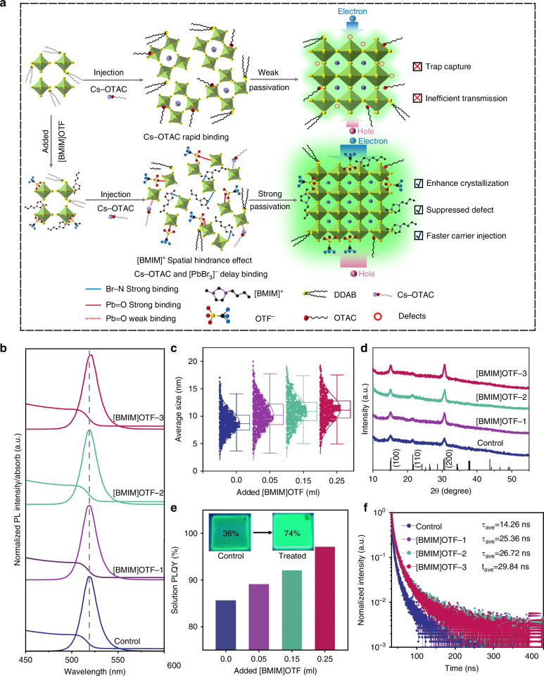
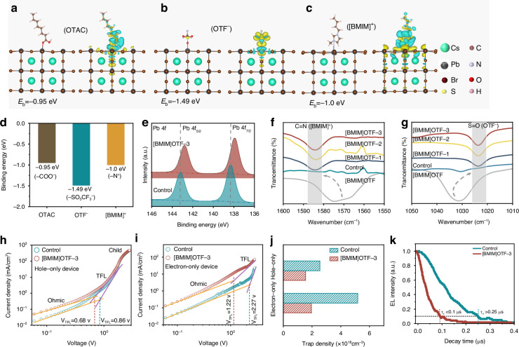
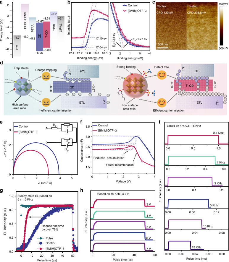
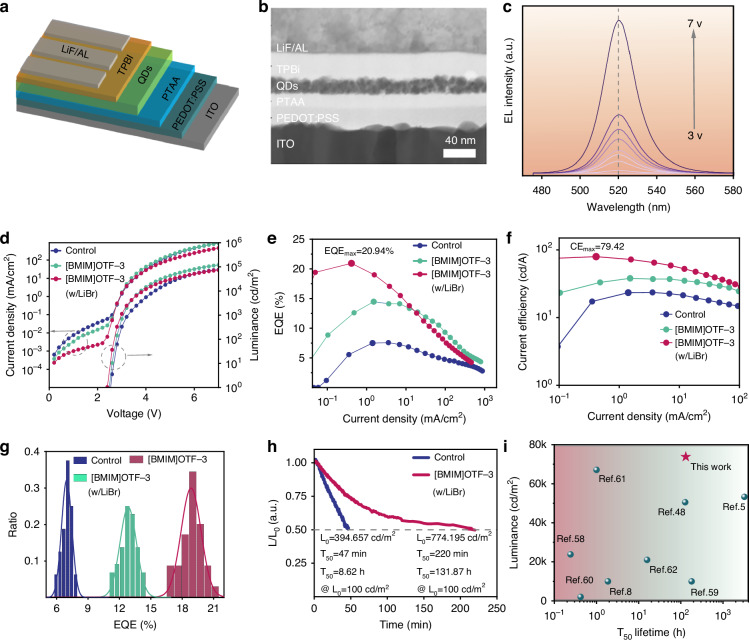
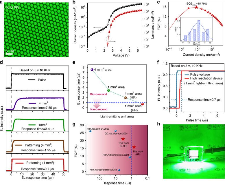
Perovskite quantum dots light-emitting diodes (PeLEDs) have been developed for next-generation high resolution display applications. However, the hindered charge injection and massive charge trapping due to the insulating and defective surface of quantum dots (QDs) usually lead to a slow rise in electroluminescence (EL) response, which makes it challenging to realize ultra-high refresh rate displays with nanosecond response. Herein, an ionic liquid 1-Butyl-3-methylimidazolium Trifluoromethanesulfonate ([BMIM]OTF) was used to enhance the crystallinity and reduce the surface area ratio of QDs, which effectively decreases defect state and injection barrier at the interface. Therefore, the rise time of EL response with steady-state is successfully reduced by over 75%. We further reduce the capacitance effect by decreasing the light-emitting unit area. Thus, ultra-high resolution (9072 pixel per inch) PeLEDs with light-emitting pixel size of 1.3 μm were realized, achieving a brightness exceeding 170,000 cd/m2 and an external quantum efficiency up to 15.79%. Moreover, it achieves nanosecond ultrafast response time under steady-state, which is the fastest response time of PeLEDs reported so far. Our work represents the most advanced performance of ultra-high-resolution PeLEDs, and provides in-depth insights into the mechanism of improving their response speed, showing significant potential in high refresh rate active display application.
© 2025. The Author(s).
Conflict of interest statement
Conflict of interest: The authors declare no competing interests.
Figures
References
-
- Levchuk, I. et al. Brightly luminescent and color-tunable formamidinium lead halide perovskite FAPbX3 (X = Cl, Br, I) colloidal nanocrystals. Nano Lett.17, 2765–2770 (2017). - PubMed
-
- Bao, C. X. et al. A multifunctional display based on photo-responsive perovskite light-emitting diodes. Nat. Electron.7, 375–382 (2024).
-
- Elkhouly, K. et al. Electrically assisted amplified spontaneous emission in perovskite light-emitting diodes. Nat. Photonics18, 132–138 (2024).
-
- Zhang, X. L. et al. Conductive colloidal perovskite quantum dot inks towards fast printing of solar cells. Nat. Energy9, 1378–1387 (2024).
-
- Wang, J. D. et al. Matched electron-transport materials enabling efficient and stable perovskite quantum-dot-based light-emitting diodes. Angew. Chem. Int. Ed.63, e202410689 (2024). - PubMed
Grants and funding
LinkOut - more resources
Full Text Sources
