

Roadmap for Photonics with 2D Materials
- PMID: 40861258
- PMCID: PMC12371959
- DOI: 10.1021/acsphotonics.5c00353
Roadmap for Photonics with 2D Materials
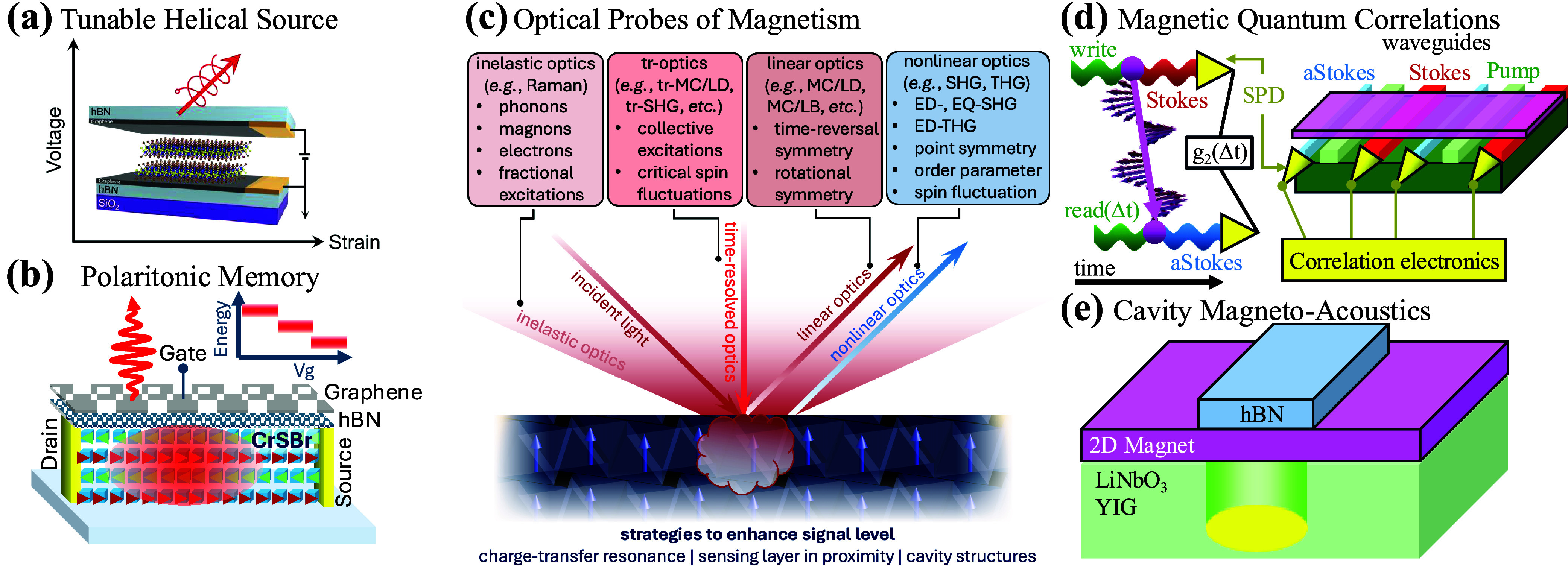
Abstract
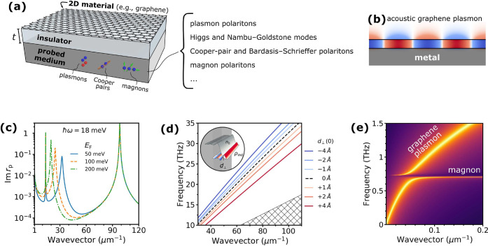
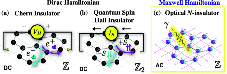
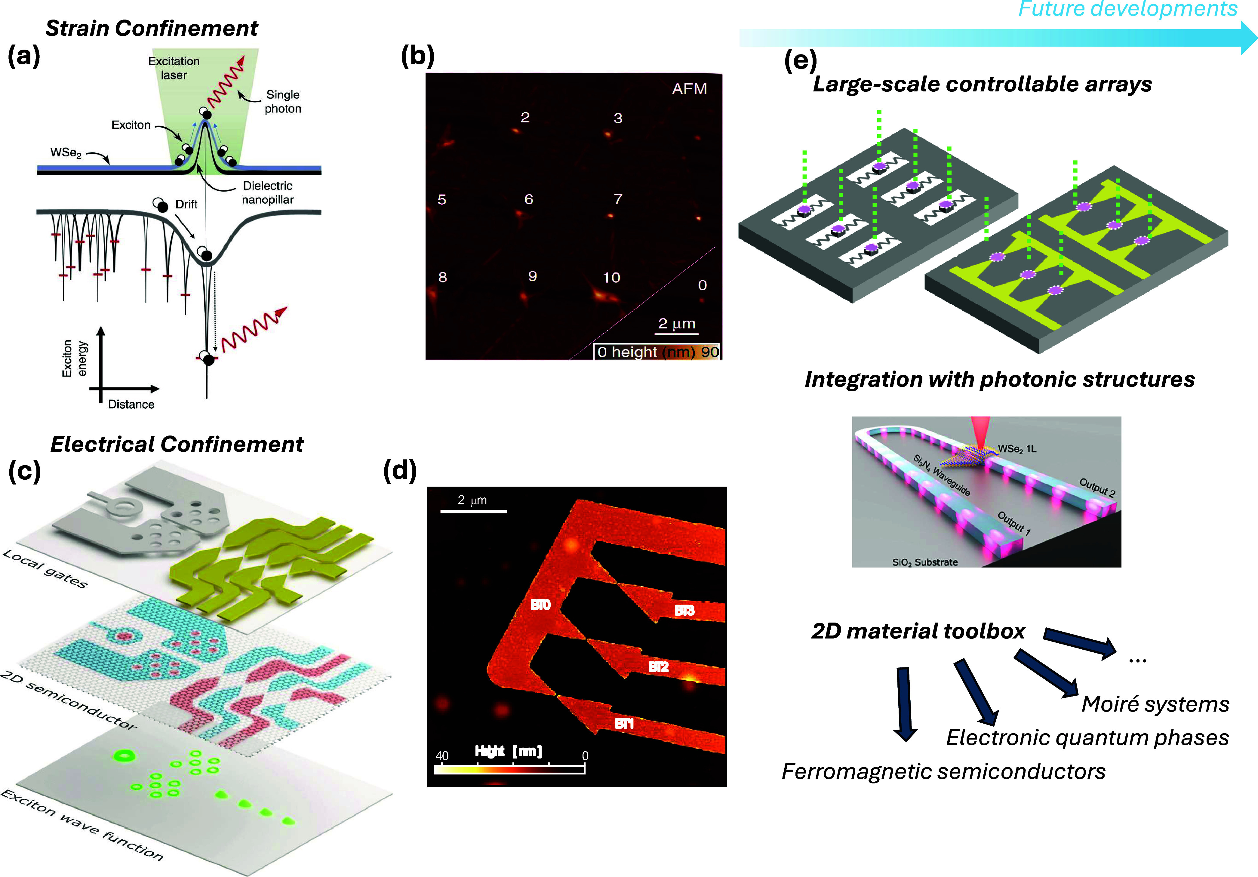
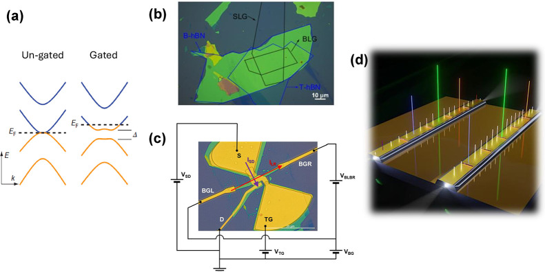
Triggered by advances in atomic-layer exfoliation and growth techniques, along with the identification of a wide range of extraordinary physical properties in self-standing films consisting of one or a few atomic layers, two-dimensional (2D) materials such as graphene, transition metal dichalcogenides (TMDs), and other van der Waals (vdW) crystals now constitute a broad research field expanding in multiple directions through the combination of layer stacking and twisting, nanofabrication, surface-science methods, and integration into nanostructured environments. Photonics encompasses a multidisciplinary subset of those directions, where 2D materials contribute remarkable nonlinearities, long-lived and ultraconfined polaritons, strong excitons, topological and chiral effects, susceptibility to external stimuli, accessibility, robustness, and a completely new range of photonic materials based on layer stacking, gating, and the formation of moiré patterns. These properties are being leveraged to develop applications in electro-optical modulation, light emission and detection, imaging and metasurfaces, integrated optics, sensing, and quantum physics across a broad spectral range extending from the far-infrared to the ultraviolet, as well as enabling hybridization with spin and momentum textures of electronic band structures and magnetic degrees of freedom. The rapid expansion of photonics with 2D materials as a dynamic research arena is yielding breakthroughs, which this Roadmap summarizes while identifying challenges and opportunities for future goals and how to meet them through a wide collection of topical sections prepared by leading practitioners.
Keywords: 2D polaritons; electro-optical modulation; excitons in van der Waals materials; layer stacking and moiré photonics; nonlinear optics; photonics with 2D materials; quantum photonics.
© 2025 The Authors. Published by American Chemical Society.
Figures


References
-
- Woessner A., Lundeberg M. B., Gao Y., Principi A., Alonso-González P., Carrega M., Watanabe K., Taniguchi T., Vignale G., Polini M., Hone J., Hillenbrand R., Koppens F. H. L.. Highly Confined Low-Loss Plasmons in Graphene-Boron Nitride Heterostructures. Nat. Mater. 2015;14:421–425. doi: 10.1038/nmat4169. - DOI - PubMed
Publication types
LinkOut - more resources
Full Text Sources