. 2025 Jul 29;16(8):882.
doi: 10.3390/mi16080882.

Composite Behavior of Nanopore Array Large Memristors

Affiliations

Composite Behavior of Nanopore Array Large Memristors

Ian Reistroffer et al. Micromachines (Basel). .

Abstract

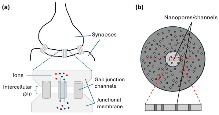
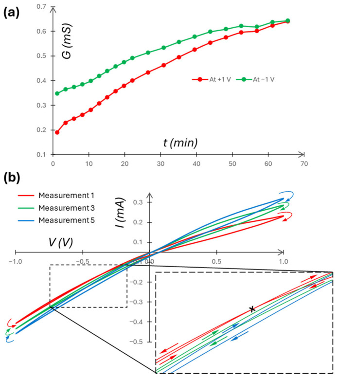
Synthetic nanopores were recently demonstrated with memristive and nonlinear voltage-current behaviors, akin to ion channels in a cell membrane. Such ionic devices are considered a promising candidate for the development of brain-inspired neuromorphic computing techniques. In this work, we show the composite behavior of nanopore-array large memristors, formed with different membrane materials, pore sizes, electrolytes, and device arrangements. Anodic aluminum oxide (AAO) membranes with 5 nm and 20 nm diameter pores and track-etched polycarbonate (PCTE) membranes with 10 nm diameter pores are tested and shown to demonstrate memristive and nonlinear behaviors with approximately 107-1010 pores in parallel when electrolyte concentration across the membranes is asymmetric. Ion diffusion through the large number of channels induces time-dependent electrolyte asymmetry that drives the system through different memristive states. The behaviors of series composite memristors with different configurations are also presented. In addition to helping understand fluidic devices and circuits for neuromorphic computing, the results also shed light on the development of field-assisted ion-selection-membrane filtration techniques as well as the investigations of large neurons and giant synapses. Further work is needed to de-embed parasitic components of the measurement setup to obtain intrinsic large memristor properties.

Keywords: membranes; memristors; nanofluidics; nanopores; rectification.


Conflict of interest statement

The authors declare no conflicts of interest.

Figures

Figure 1
Figure 1
(a) Electrical synapses with gap junction channels allowing a direct communication between the cytoplasm of the two coupled cells via anions (red) and cations (black) [17]. (b) A nanoporous membrane with many channels in parallel. The number of active pores can be reduced by blocking membrane surface, such as the dark grey areas. The inset shows the nanochannels from a slice cross-section of the membrane.
Figure 2
Figure 2
(a) A photograph of the experimental setup. A SourceMeter supplies a voltage to the Ag/AgCl electrode on the left-hand side and measures the current through the electrode on the right-hand side. (b) A schematic (not to scale) of the components inside the membrane holder. Both electrode faces are positioned a distance d (about 10 μm) from either side of the membrane. In the case of PCTE and AAO isotropic membranes, only a single layer (AL) is present; in the case of AAO anisotropic membranes, an additional layer (SL) is present with its own unique width, pore diameter, and pore density. The volume of the cL and cH solutions are 0.79 and 0.3 mL, respectively.
Figure 3
Figure 3
(a) A photograph of the 13 mm diameter AAO isotropic membrane held by tweezers. (bd) SEM scans of the membrane showing (b) the top surface (20 nm diameter pores/channels), (c) the bottom surface, and (d) a cross-section slice (all used with permission by InRedox, Longmont, CO, USA). The white inset diagram in (c) illustrates a potential slight asymmetry of the top and bottom conical openings due to tapering.
Figure 4
Figure 4
(a) Schematic representation of a single nanochannel connecting reservoirs of cL solution (light grey, low concentration) and cH solution (dark grey, high concentration). The EDL is represented in the red enclosure, corresponding to an enrichment of anions that have migrated toward the positively charged channel walls. (b) A diagram of the electrical measurement circuit. Depending on the measurement, either the SourceMeter or AD2 device may be connected to the system. Using the AD2, a parasitic capacitance of 1.8 pF is in parallel with the system. Cp is parasitic capacitance across the nanopore array. REE is the resistance of the electrode–electrolyte interfaces.
Figure 5
Figure 5
(a,c) Typical I/V measurements and (b,d) their associated G/V measurements using an AAO Isotropic membrane (with pore size of 20 nm and 50-μm channel length), applying a 1 V amplitude signal with 0.1 Hz frequency, using KCl electrolyte. KCl concentrations are (a,b) cL = cH = 0.1 mM and (c,d) cL = 0.1 mM and cH = 100 mM. The inset in (c) shows the memristive self-crossing point. In all figures, arrows indicate scan direction.
Figure 6
Figure 6
Time-dependent measurements using 0.1|100 mM KCl, an AAO isotropic membrane, and a ±1 V, 0.1 Hz signal. (a) Conductance over time measured at both amplitude peaks (at +1 V in red) and troughs (at −1 V in green). (b) Multiple measurements over time. Measurement 1 (i.e., cycle 2 of scan 1) begins 1 min 10 s after solution injection, with successive measurements beginning after 2 min, 20 s gaps. The inset magnifies the I/V self-crossing point of measurement 1 (marked by the x). The arrows indicate scan direction. The arrows indicate scan direction, colored according to their associated measurement.
Figure 7
Figure 7
(a) I/V plot of varying signal frequencies. Scan directions are indicated by arrows and self-crossing points are indicated by an “x”, both colored according to their associated measurement. (b) Conductance taken at the peaks and troughs of the voltage signal, measured over time for each of the three frequencies. Measurement number is constant for comparable statistics. Both use 0.1|100 mM KCl, an AAO Isotropic membrane, and a 1 V signal amplitude.
Figure 8
Figure 8
I/V dependence using different device parameters. In all cases, a voltage of ±1 V, 0.1 Hz is applied. Arrows indicate scan direction and an “x” indicates a self-crossing point, both colored according to the corresponding measurement. (a) (Left) varying cH while holding cL constant at 0.1 mM KCl, and (right) same plot with a truncated y-axis to show more clearly the 0.1|0.1 mM, 0.1|1 mM, and 0.1|10 mM measurements. (b) Varying the membrane type; all measurements trend in the same direction, and all have a self-crossing point (not marked) in the third quadrant. (c) Varying the applied voltage amplitude.
Figure 9
Figure 9
I/V measurements using two membrane devices in series with a single membrane device as reference. All devices use 0.1|100 mM KCl and a 0.1 Hz signal. (a) Photographs of the measurement setup: (red/top) a single memristor, (green/middle) two memristors in series, both with the orientation of the single device, and (blue/bottom) two devices in series, where the second is in the opposite orientation as the first. (b) Measurements of all devices using AAO Isotropic membranes in each holder. (c) Measurements of all devices, with AAO Anisotropic membranes in each holder and using a signal amplitude of 2 V for both double-membrane devices and a 1 V amplitude for the single-membrane device. (d) Measurements of all devices, with AAO Anisotropic membranes in each holder and using a signal amplitude of 50 mV.

Similar articles

References

    1. Islam R., Li H., Chen P.-Y., Wan W., Chen H.-Y., Gao B., Wu H., Yu S., Saraswat K., Wong H.P. Device and materials requirements for neuromorphic computing. J. Phys. D Appl. Phys. 2019;52:113001. doi: 10.1088/1361-6463/aaf784. - DOI
    1. Aguirre F., Sebastian A., Le Gallo M., Song W., Wang T., Yang J.J., Lu W., Chang M.-F., Ielmini D., Yang Y. Hardware implementation of memristor-based artificial neural networks. Nat. Commun. 2024;15:1974. doi: 10.1038/s41467-024-45670-9. - DOI - PMC - PubMed
    1. Hodgkin A.L., Huxley A.F. A quantitative description of membrane current and its application to conduction and excitation in nerve. J. Physiol. 1952;117:500. doi: 10.1113/jphysiol.1952.sp004764. - DOI - PMC - PubMed
    1. Chua L. Memristor-the missing circuit element. IEEE Trans. Circuit Theory. 1971;18:507–519. doi: 10.1109/TCT.1971.1083337. - DOI
    1. Strukov D.B., Snider G.S., Stewart D.R., Williams R.S. The missing memristor found. Nature. 2008;453:80–83. doi: 10.1038/nature06932. - DOI - PubMed

Grants and funding

LinkOut - more resources