

Multimodal characterization of Te inclusions in Cd1-xZnxTe and Cd1-xZnxTe1-ySey for gamma and X-ray detectors
- PMID: 40885751
- PMCID: PMC12398591
- DOI: 10.1038/s41598-025-15132-3
Multimodal characterization of Te inclusions in Cd1-xZnxTe and Cd1-xZnxTe1-ySey for gamma and X-ray detectors
Abstract
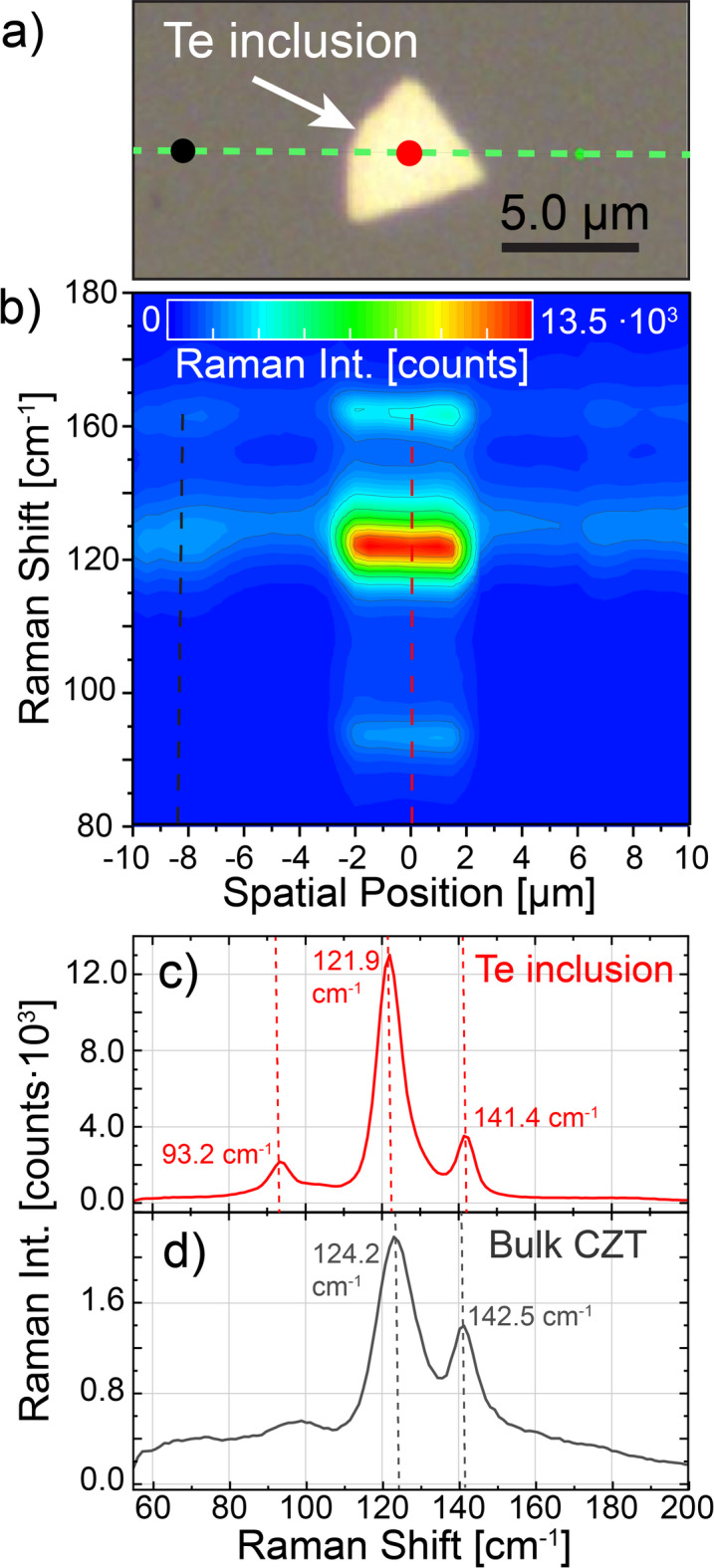
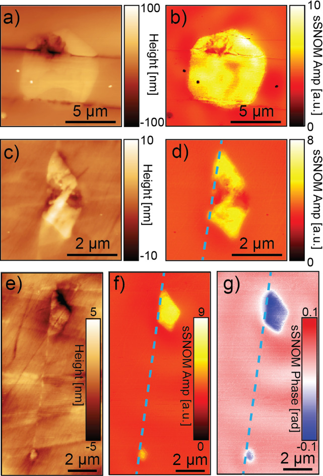
While CdZnTe (CZT) and CdZnTeSe (CZTS) semiconductors have emerged as compounds for room-temperature gamma and X-ray detection materials, they continue to be constrained by the formation of Te-inclusion defects generated during the growth and post-growth phases of the material, which adversely affect the detector performance. We demonstrate the utility of multimodal microscopic imaging and analysis for the characterization of the optical and electronic properties of Te inclusions in CZT and CZTS crystals at both micron and nanometer length scales. Having first identified regions with micron-scale Te inclusions using confocal Raman microscopy techniques, optically coupled infrared scattering near-field optical microscopic mapping was performed to map the distribution of these inclusions with nanometer spatial resolution and correlate the presence of Te inclusions in the matrix with other properties. Kelvin probe force microscopy was then utilized to characterize the variations of the work function associated with the presence of Te inclusions. Here, we observe an increase of ~ 240 mV in the work function associated with Te inclusions compared to the bulk CZT/CZTS crystals. Additionally, we observe that individual bulk grains in CZT can exhibit slight potential variations. Our findings develop a portrait of the charge trapping mechanisms in CZT and CZTS that act to degrade detector performance, while the demonstration of these combined microscopy techniques provides a new analytical tool that can be utilized for further optimization of the detector performance for these semiconducting compounds.
© 2025. The Author(s).
Conflict of interest statement
Competing interests: The authors declare no competing interests.
Figures


References
-
- Schieber, M. et al. Material properties and room-temperature nuclear detector response of wide bandgap semiconductors. Nucl. Instrum. Methods Phys. Res. Sect. A: Accel. Spectrom. Detect. Assoc. Equip.377, 492–495. 10.1016/0168-9002(96)00030-7 (1996).
-
- Luan, L., Lv, H., Gao, L., He, Y. & Zheng, D. Preparation and properties of hemispherical CdMnTe nuclear radiation detectors. Nucl. Instrum. Methods Phys. Res. Sect. B: Beam Interact. Mater. At.471, 42–47. 10.1016/j.nimb.2020.03.018 (2020).
-
- Sun, M. et al. Material properties and device performance of CdSe radiation detectors. Nucl. Instrum. Methods Phys. Res. Sect. A: Accel. Spectrom. Detect. Assoc. Equip.10.1016/j.nima.2020.163487 (2020).
-
- Kishore, V., Saraswat, V. K., Saxena, N. S. & Sharma, T. P. Structural and electrical measurements of CdZnSe composite. Bull. Mater. Sci.28, 431–436. 10.1007/bf02711232 (2005).
Grants and funding
- DE-NA0003980/Department of Energy (DoE), Office of the National Nuclear Security Administration (NNSA) Minority Serving Institutions Internship Program
- DE-NA0003980/Department of Energy (DoE), Office of the National Nuclear Security Administration (NNSA) Minority Serving Institutions Internship Program
- DE-NA0003980/Department of Energy (DoE), Office of the National Nuclear Security Administration (NNSA) Minority Serving Institutions Internship Program
- DE-NA0003980/Department of Energy (DoE), Office of the National Nuclear Security Administration (NNSA) Minority Serving Institutions Internship Program
- DE-NA0003980/Department of Energy (DoE), Office of the National Nuclear Security Administration (NNSA) Minority Serving Institutions Internship Program
- DE-NA0003980/Department of Energy (DoE), Office of the National Nuclear Security Administration (NNSA) Minority Serving Institutions Internship Program
- DE-NA0003980/Department of Energy (DoE), Office of the National Nuclear Security Administration (NNSA) Minority Serving Institutions Internship Program
- DE-NA0003980/Department of Energy (DoE), Office of the National Nuclear Security Administration (NNSA) Minority Serving Institutions Internship Program
- DE-NA0003980/Department of Energy (DoE), Office of the National Nuclear Security Administration (NNSA) Minority Serving Institutions Internship Program
- DE-NA0003980/Department of Energy (DoE), Office of the National Nuclear Security Administration (NNSA) Minority Serving Institutions Internship Program
- 89233218CNA000001/Department of Energy
- 89233218CNA000001/Department of Energy
- 89233218CNA000001/Department of Energy
- 89233218CNA000001/Department of Energy
LinkOut - more resources
Full Text Sources
