. 2025 Sep 1;16(1):8178.
doi: 10.1038/s41467-025-62635-8.

Integrated lithium niobate photonic computing circuit based on efficient and high-speed electro-optic conversion

Affiliations

Integrated lithium niobate photonic computing circuit based on efficient and high-speed electro-optic conversion

Yaowen Hu et al. Nat Commun. .

Abstract

The surge in artificial intelligence applications calls for scalable, high-speed, and low-energy computation methods. Computing with photons is promising due to the intrinsic parallelism, high bandwidth, and low latency of photons. However, current photonic computing architectures are limited by the speed and energy consumption associated with electronic-to-optical data transfer, i.e., electro-optic conversion. Here, we demonstrate a thin-film lithium niobate (TFLN) computing circuit that addresses this challenge, leveraging both highly efficient electro-optic modulation and the spatial scalability of TFLN photonics. Our circuit is capable of computing at 43.8 GOPS/channel while consuming 0.0576 pJ/OP, and we demonstrate various inference tasks with high accuracy, including the classification of binary data and complex images. Heightening the integration level, we show another TFLN computing circuit that is combined with a hybrid-integrated distributed-feedback laser and heterogeneous-integrated modified uni-traveling carrier photodiode. Our results show that the TFLN photonic platform holds promise to complement silicon photonics and diffractive optics for photonic computing, with extensions to ultrafast signal processing and ranging.


Conflict of interest statement

Competing interests: L.H., Y.W., K.L., M.Z., and M.L. are involved in developing lithium niobate technologies at HyperLight Corporation. The remaining authors declare no competing interests.

Figures

Fig. 1
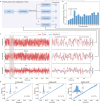
Fig. 1. Photonic computing accelerator on thin-film lithium niobate.
a Concept of photonic computing accelerators. Data stored in the electronic system (e.g. a computer) are sent to the photonic accelerator at high rates and are converted into the optical domain. Parallel computations are then performed by the accelerator and results are returned to the electronic system. b Illustration of the photonic computing working principle. Continuous-wave light passes through two cascaded amplitude modulators (AMs) which sequentially encode elements of x and a onto the amplitude of light, effectively performing element-wise multiplication of the two vectors. The components contributing to xa are read out by optical-to-electronic conversion using a low-noise and high-speed detector, and electronic summation of these components finally yields xa. c The vision for a fully integrated computing core based on TFLN photonics, consisting of laser, detectors, and TFLN modulators for high-speed and energy-efficient EO conversion and computation. An input vector is first encoded in the time domain of the optical field through an amplitude modulator and then fanned-out into N spatial channels (N=16 in this figure) to leverage massive spatial parallelism. In each channel, another amplitude modulator is used to multiply weights with the input vector. Finally, detectors convert the multiplication results back into electronic signals.
Fig. 2
Fig. 2. Integrated thin-film lithium niobate photonic circuit implementation of computing core.
a Optical microscope and scanning electron microscope images of the building blocks used in the integrated TFLN circuit: waveguide array (top left) for signal routing; grating coupler (top center) for efficient in- and out-coupling of light; ring resonator (top right) for evaluating the propagation loss and etch quality; fan-out splitter tree (bottom center) to distribute light into distinct spatial channels; microwave transmission line (bottom left) for delivering efficient EO modulation; and on-chip terminator (bottom right) for high-quality microwave impedance matching. b Optical microscope image of seven weight modulators in the TFLN accelerator. c Full image of one computing core (our circuit contains two such computing cores on the same chip). d Scanning electron microscope image of a high-quality waveguide featuring low propagation loss, enabling low optical energy consumption for the entire circuit. e Cross-section illustration of the TFLN circuit, including gold, nickel-chromium (NiCr), lithium niobate, silicon dioxide, and silicon. d=100nm, w=1.5μm, h0=300nm, h1=1.0μm, h2=800nm, t=300nm, t1=4.7μm, t2=525μm. f Measured terminator resistance vs. length. g EO forward transmission (S21 EO) and electric-electric input reflection (S11EE) response of the modulators in our circuit. Our circuit features a combined total of 31 spatial channels (32 designed, but one failed during the fabrication process). All modulators have a bandwidth beyond 40 GHz (measurement limited by our detector bandwidth). h Representative VπL of the modulators (length 1 cm) in our circuit.
Fig. 3
Fig. 3. High-speed and energy-efficient photonic computing on thin-film lithium niobate.
a Two-dimensional illustration of the photonic computing core structure. b Computational accuracy for different channels in one computing core. The differences in accuracy between channels is minimal though can be further reduced through fine tuning of the system operational parameters. c Example waveforms of a temporally-multiplexed computing operation between two random vectors x and a with 22.8 ps/symbol. Deviations between theory and experiment can be attributed to limited system bandwidth and residual inaccuracy in time delay between x and a. Since the final MVM result is a summation of the data trace, it averages out these deviations and further reduces the error. d Computational accuracy vs. energy consumption by varying the optical power, showing a lowest energy consumption of 0.0576 pJ/OP at 22.8 ps/symbol, while still maintaining computational accuracy. The inset gives error of the computation (Error = Measured-Expected). The σ is the standard deviation of the error.
Fig. 4
Fig. 4. Photonic binary classification.
a Illustration of binary classification conducted over a data set consisting of two-dimensional vectors x=x1,x2T, where each vector is labeled positive or negative based on the exclusive-or condition. To infer the label of some x, a number of computing operations are carried out by our photonic accelerator to compute xTQx followed by electronic nonlinear activation. Here, Q is a pre-trained kernel matrix and nonlinearity is electronically applied. Accuracy of inference thus depends on the accuracy of photonic computations. b Classification of 400 randomly selected x in the problem space, colored by their photonics-inferred positive (blue) and negative (red) labels. c Comparison between photonic and electronic classification results over the 400-vector test set, which shows good agreement between photonic and electronic computing. The photonic circuit (electronic computer) achieves a classification accuracy of 93.8% (93.5%).
Fig. 5
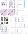
Fig. 5. Photonic computing for fully-connected layers of photonic neural networks.
a Classification of an MNIST handwritten digit. The image is flattened into a single vector encoded in the time domain. An example image (number six) is shown on the left. A two-layer photonic neural network is used to perform the classification task (center). The photonic computing result at the end of the network is then sent back to the computer to perform a nonlinear activation (right). The final classification results agree well with the electronically computed result. b Statistics of MNIST handwritten digit recognition. 500 MNIST images are selected as the test set and processed. The confusion matrices show a classification accuracy of 88% using our circuit (92% using electronic computer). c Stability. The computing core is programmed to continuously run identical computing tasks over 20 h, experiencing minimal fluctuations of 0.04%. d Real image classification. Images resembling real-life objects are selected from the CIFAR-10 database and classified using a convolutional neural network. The images are preprocessed through convolution layers, flattened into vectors, and then sent into our circuit to be classified by the remaining fully-connected layers (bottom left). Nine example figures including a truck, cat, bird, automobile, frog, deer, ship, airplane, and horse (top left), together with the classification results (right) are shown, indicating our photonic computing circuit can accurately process large, multi-layer networks.
Fig. 6
Fig. 6. Hybrid- and heterogenous- integrated TFLN photonic computing circuit.
a Wafer-scale fabrication of computing cores comprising a TFLN photonic computing circuit. b Chiplets of TFLN computing cores from the wafer-scale process. c, Measurement setup for characterizing the hybrid- and heterogeneous-integrated system: light from a hybrid-integrated DFB laser source is butt-coupled to the TFLN computing core, while a heterogeneous-integrated MUTC-PD is used to perform optical-to-electronic conversion of the computing signal (the electrical signal is extracted by contact probes). d Optical microscope images of essential building blocks used for the integrated TFLN circuit similar to Fig. 2a, except bilayer-taper edge couplers (top middle) are employed as a low-loss interface between the TFLN waveguide mode and the DFB waveguide mode. e Schematic of a single channel integrated system. f Optical microscope image of DFB laser and 2-D simulation of the DFB waveguide mode. P (N): positively- (negatively-) doped region; QW: quantum well. g Optical microscope image of TFLN photonic computing circuit, with an array of cascaded amplitude modulators (left) and an array of MUTC-PDs (right). h Optical microscope image of MUTC-PD and schematic of its cross section. i DFB output power measured by an integrating sphere vs. injection current, with about 50 mA current threshold and 0.25 W/A slope efficiency. j MUTC-PD dark current vs. bias voltage. For high-speed operation, a reverse-bias of −2 V is held for all measurements. k Example waveforms of a temporally multiplexed computing operation between two random vectors x and a with 96.8 ps/symbol (10.33 GOPS per channel). l Computational accuracy σ, as previously defined, vs. computing energy consumption as the DFB output power is varied. Three energy consumptions are evaluated based on experimental conditions provided DFB injection currents of 85, 125, and 150 mA, respectively.

References

    1. Yao, P. et al. Fully hardware-implemented memristor convolutional neural network. Nature577, 641–646 (2020). - PubMed
    1. Wan, W. et al. A compute-in-memory chip based on resistive random-access memory. Nature608, 504–512 (2022). - PMC - PubMed
    1. Wright, L. G. et al. Deep physical neural networks trained with backpropagation. Nature601, 549–555 (2022). - PMC - PubMed
    1. Shen, Y. et al. Deep learning with coherent nanophotonic circuits. Nat. Photonics11, 441–446 (2017).
    1. Lin, X. et al. All-optical machine learning using diffractive deep neural networks. Science361, 1004–1008 (2018). - PubMed

LinkOut - more resources