Review
. 2025 Aug 27:16:1428-1498.
doi: 10.3762/bjnano.16.104. eCollection 2025.

Laser processing in liquids: insights into nanocolloid generation and thin film integration for energy, photonic, and sensing applications

Affiliations
Review

Laser processing in liquids: insights into nanocolloid generation and thin film integration for energy, photonic, and sensing applications

Akshana Parameswaran Sreekala et al. Beilstein J Nanotechnol. .

Abstract

Nanoparticles in their pure colloidal form synthesized by laser-assisted processes such as laser ablation/fragmentation/irradiation/melting in liquids have attained much interest from the scientific community because of their specialties like facile synthesis, ultra-high purity, biocompatibility, colloidal stability in addition to other benefits like tunable size and morphology, crystalline phases, new compounds and alloys, and defect engineering. These nanocolloids are useful for fabricating different devices mainly with applications in optoelectronics, catalysis, sensors, photodetectors, surface-enhanced Raman spectroscopy (SERS) substrates, and solar cells. In this review article, we describe different methods of nanocolloidal synthesis using laser-assisted processes and corresponding thin film fabrication methods, particularly those utilized for device fabrication and characterization. The four sections start with an introduction to the common laser-assisted synthesis for nanocolloids and different methods of thin film fabrication using these nanocolloids followed by devices fabricated and characterized for applications including photovoltaics, photodetectors, catalysis, photocatalysis, electrochemical/photoelectrochemical sensors, hydrogen/oxygen evolution, SERS sensors and other types of devices reported so far. The last section explains the challenges and further scope of these devices from laser-generated nanocolloids.

Keywords: HER/OER/water splitting; laser synthesis of nanomaterials; nanocolloids to thin films; photocatalysis; photovoltaics and photodetection; surface-enhanced Raman spectroscopy (SERS).


Figures

Figure 1
Figure 1
A visual roadmap tracing key advancements in thin film deposition methods and laser-based material processing [3]. All graphical elements including road, human beings, pinpoints and flag: ©Pooja Raveendran Nair and Akshana Parameswaran Sreekala via Canva.com.
Figure 2
Figure 2
Morphologies of Au NPs prepared by PLA in various solvents. Figure 2 was used with permission of The Royal Society of Chemistry, from [16] (“What controls the composition and the structure of nanomaterials generated by laser ablation in liquid solution?” by V. Amendola and M. Meneghettia, Phys. Chem. Chem. Phys., vol. 15, issue 9, © 2013); permission conveyed through Copyright Clearance Center, Inc., This content is not subject to CC BY 4.0.
Figure 3
Figure 3
(a) Influence of the wavelength on the concentration of fragmented particles after 5 min of irradiation with UV (266 nm), visible (532 nm), and IR (1064 nm) at 120 mJ. (b) Photoluminescence spectra and (c) Tauc plots for the ZnO nanoparticles both before (orange lines) and after (blue lines) PLFL processing. Figure 3a was reprinted from [31], Journal of Colloid and Interface Science, vol. 357, by C. Chubilleau; B. Lenoir; S. Migot; A. Dauscher, “Laser fragmentation in liquid medium: A new way for the synthesis of PbTe nanoparticles”, pages 13–17, Copyright (2011), with permission from Elsevier. This content is not subject to CC BY 4.0. Figure 3b,c were reproduced from [33] (© 2020 K. Charipar et al., published by MDPI, distributed under the terms of the Creative Commons Attribution 4.0 International License, https://creativecommons.org/licenses/by/4.0).
Figure 4
Figure 4
SEM images of Ba5Ta4O15 and BaTaOxNy-zp powders with increasing number of laser fragmentation passages. The arrows show the BaCO3 secondary phase. Figure 4 was reprinted from [40], Applied Surface Science, vol. 510, by F. Haydous; F. Waag; W. Si; F. Li; S. Barcikowski; B. Gökce; T. Lippert, “The effect of downstream laser fragmentation on the specific surface area and photoelectrochemical performance of barium tantalum oxynitride”, article no. 145429, Copyright (2020), with permission from Elsevier. This content is not subject to CC BY 4.0.
Figure 5
Figure 5
(a, b) SEM morphologies and size distribution of Ge nanoparticles obtained by laser ablation in water (c, d) SEM morphologies and size distribution of Ge submicrometer spheres synthesized by post laser irradiation of the LAL-synthesized particles. Figure 5 was reproduced from [53], (© 2017 D. Zhang et al., published by Springer Nature, distributed under the terms of the Creative Commons Attribution 4.0 International License, https://creativecommons.org/licenses/by/4.0).
Figure 6
Figure 6
(a) EDS mapping images of particles obtained by different laser irradiation times from the Au raw particle solution. Particle size dependence of laser fluence required to melt a single particle of Au, Fe3O4, and Fe2O3 calculated based on Mie theory and adiabatic assumption (b) 532 nm. (c) 355 nm. Figure 6 was reproduced from [61] (© 2019 H. Fuse et al., published by MDPI, distributed under the terms of the Creative Commons Attribution 4.0 International License, https://creativecommons.org/licenses/by/4.0).
Figure 7
Figure 7
FESEM images of the submicrometer spheres obtained by the modest laser irradiation of commercial (a) ZnO, (b) WO3, (c) Cu, and (d) Fe NPs. Insets: magnified SEM images. (e) Evolution of average size of QDs with laser irradiation. The sharp decrease in the first stage is attributed to the rapid collapse and transformation into plasma, and the subsequent slight increase in the second stage corresponds to the growth of QDs. The selective pulsed heating involved in pulsed laser irradiation of colloidal nanoparticles. (f) Temporal discontinuity: pulsed heating and subsequent quenching, and (g) spatial discontinuity: only the particles are heated, not the solvent. Figure 7a–d,f,g was reproduced from [42], H. Wang et al., “Selective Pulsed Heating for the Synthesis of Semiconductor and Metal Submicrometer Spheres”, Angewandte Chemie - International Edition with permission from John Wiley and Sons. Copyright © 2010 WILEY‐VCH Verlag GmbH & Co. KGaA, Weinheim. This content is not subject to CC BY 4.0. Figure 7e was adapted with permission from [34], Copyright 2011 American Chemical Society. This content is not subject to CC BY 4.0.
Figure 8
Figure 8
SEM of silicon particles (a, b) before and (c, f) after laser irradiation (460 mJ/pulse cm2, 30 min). Images (a), (c), and (e) are the morphologies without milling and (b), (d), and (f) are those with milling. Images (e) and (f) are magnified images of (c) and (d), respectively. (g) Absorption of silicon particles in ethanol before and after milling. Figure 8 was reprinted with permission from [48], Copyright 2011 American Chemical Society. This content is not subject to CC BY 4.0.
Figure 9
Figure 9
General schematics of the different techniques of thin film fabrication using nanocolloids synthesized by LPL. The photodetector device figure used at the center was reproduced with permission from [99] (© 2021 N. S. Rohizat et al., published by Springer Nature, distributed under the terms of the Creative Commons Attribution 4.0 International License, https://creativecommons.org/licenses/by/4.0).
Figure 10
Figure 10
(a) Photograph of a typical spin-coating operation and high-speed images showing application of a solution of MEHPPV to a rotating substrate and film formation. The timing of the images (from left to right) after impact of the first drop is: t = 17, 100, 137, and 180 ms. (b) Photos of the SnS nanocolloids prepared by PLAL using laser of wavelength (i) 532 nm, (ii) 1064 nm and (c) their thin films by spin coating (I, II) SnS as-prepared (AP), (III, IV) annealed at 350 °C, (V, VI) annealed at 450 °C, (d) XRD diffractogram of CdS nanoropes, Si wafer p-type, and CdS film on Si (111) substrate prepared by spin-coating. Figure 10a was reprinted from [112], Solar Energy Materials and Solar Cells, vol. 93, by F. C. Krebs, “Fabrication and processing of polymer solar cells: A review of printing and coating techniques”, pages 394–412, Copyright (2009), with permission from Elsevier. This content is not subject to CC BY 4.0. Figure 10b,c was reprinted from [104], Colloids and Surfaces A: Physicochemical and Engineering Aspects, vol. 639, by A. P. Sreekala; B. Krishnan; R. F. C. Pelaes; D. A. Avellaneda; M. I. M. Palma; S. Shaji, “Tin sulfide thin films by spin coating of laser ablated nanocolloids for UV–Vis–NIR photodetection”, article no. 128382, Copyright (2022), with permission from Elsevier. This content is not subject to CC BY 4.0. Figure 10d was reproduced from [109] (© 2023 F. H. Alkallas et al., published by MDPI, distributed under the terms of the Creative Commons Attribution 4.0 International License, https://creativecommons.org/licenses/by/4.0).
Figure 11
Figure 11
(a) Peak intensity ratio IUV/Ivis of UV near band edge emission to visible deep-level emission of ZnO colloidal solutions drop-cast onto Si wafers. (b) 3D AFM image of ZnO NPs drop-cast on glass substrate. (c) Schematic of centrifuged Ag NP ink drop-cast on a glass slide. (d) In situ resistance vs temperature during heat-treatment of the centrifuged Ag ink drop-cast layer. Figure 11a was reprinted from [115], Materials Science in Semiconductor Processing, vol. 109, by W. Chen; C. Yao; J. Gan; K. Jiang; Z. Hu; J. Lin; J. Sun; J. Wu, “ZnO colloids and ZnO nanoparticles synthesized by pulsed laser ablation of zinc powders in water”, article no. 104918, Copyright (2020), with permission from Elsevier. This content is not subject to CC BY 4.0. Figure 11b was reproduced from [119] (© 2019 B. Ali and Al-Mustansiriyah Journal of Science, published by Al-Mustansiriyah Journal of Science, distributed under the terms of the Creative Commons Attribution-NonCommercial 4.0 International License, https://creativecommons.org/licenses/by-nc/4.0/). This content is not subject to CC BY 4.0. Figure 11c,d was reprinted from [120], Nano-Structures & Nano-Objects, vol. 29, by É. McCarthy; S. P. Sreenilayam; O. Ronan; H. Ayub; R. McCann; L. McKeon; K. Fleischer; V. Nicolosi, “Silver nanocolloid generation using dynamic Laser Ablation Synthesis in Solution system and drop-casting”, article no. 100841, Copyright (2022), with permission from Elsevier. This content is not subject to CC BY 4.0.
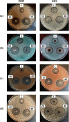
Figure 12
Figure 12
(a) Photograph showing the doctor blade technique. (b) Images of ZnO powders after 60 and 90 min of laser irradiation and their films prepared by doctor blade technique. (c) SEM images of the ZnO films deposited by doctor blade method and annealed at 400 °C. Figure 12a was reprinted from [112], Solar Energy Materials and Solar Cells, vol. 93, by F. C. Krebs, “Fabrication and processing of polymer solar cells: A review of printing and coating techniques”, pages 394–412, Copyright (2009) with permission from Elsevier. This content is not subject to CC BY 4.0. Figure 12b was reprinted from [125], Applied Surface Science, vol. 567, by S. S. Kanakkillam; B. Krishnan; S. S. Guzman; J. A. A. Martinez; D. A. Avellaneda; S. Shaji, “Defects rich nanostructured black zinc oxide formed by nanosecond pulsed laser irradiation in liquid”, article no. 150858, Copyright (2021), with permission from Elsevier. This content is not subject to CC BY 4.0. Figure 12c was reprinted from [126], Thin Solid Films, vol. 597, by C. Sima; C. Grigoriu; O. Toma; S. Antohe, “Study of dye sensitized solar cells based on ZnO photoelectrodes deposited by laser ablation and doctor blade methods”, pages 206–211, Copyright (2015), with permission from Elsevier. This content is not subject to CC BY 4.0.
Figure 13
Figure 13
Schematic representation of an ultrasonic spray deposition setup.
Figure 14
Figure 14
Structure and morphology of the Au sample prepared by EPD. (a) XRD result (b, c) FESEM images with different magnifications. (d) TEM image of the product scraped from the sample. (e) Schematic illustration of cathodic EPD of the nanoparticles in an electrical field. Figure 14a–d was used with permission of The Royal Society of Chemistry, from [131] (“Au nanochain-built 3D netlike porous films based on laser ablation in water and electrophoretic deposition” by H. He et al., Chem. Commun., vol. 46, issue 38, © 2010); permission conveyed through Copyright Clearance Center, Inc. This content is not subject to CC BY 4.0. Figure 14e was adapted with permission from [134], Copyright 2012 American Chemical Society. This content is not subject to CC BY 4.0.
Figure 15
Figure 15
Illustration showing nano materials used for the fabrication of different devices using LPL. All graphical elements including tree and the leaves: ©Jithin Kundalam Kadavath via Canva.com.
Figure 16
Figure 16
(a) IV EQE characteristics measured for a CIGS solar cell on a Mo metal sheet. The inset photo and illustration show the solar cell and its device structure, respectively. (b) SEM images of the CH3NH3PbI3-PbS films prepared using the PbS colloids synthesized for different ablation times as marked. Also, pristine sample CH3NH3PbI3 (as prepared) is given. (c) Solar cell JV curves under dark and light of the structure glass/FTO/CdS/Sb2S3/CAS where the CAS layer is deposited by spraying laser ablated CAS nanocolloids. The schematic of the film stack structure with a circuit diagram is also included. Figure 16a was adapted with permission from [134], Copyright (2012) American Chemical Society. This content is not subject to CC BY 4.0. Figure 16b was reprinted from [130], Applied Surface Science, vol. 476, by S. Shaji; V. Vinayakumar; B. Krishnan; J. Johny; S. S. Kanakkillam; J. M. F. Herrera; S. S. Guzman; D. A. Avellaneda; G. A. C. Rodriguez; J. A. A. Martinez, “Copper antimony sulfide nanoparticles by pulsed laser ablation in liquid and their thin film for photovoltaic application”, pages 94–106, Copyright (2019) with permission from Elsevier. This content is not subject to CC BY 4.0. Figure 16c was reprinted from [139], Applied Surface Science, vol. 508, by D. A. A. Leal; S. Shaji; D. A. Avellaneda; J. A. A. Martínez; B. Krishnan, “In situ incorporation of laser ablated PbS nanoparticles in CH3NH3PbI3 films by spin-dip coating and the subsequent effects on the planar junction CdS/CH3NH3PbI3 solar cells”, article no. 144899, Copyright (2020) with permission from Elsevier. This content is not subject to CC BY 4.0.
Figure 17
Figure 17
(a) Optical top-view image of the B4C/p-Si heterojunction photodetector. (b) Optical absorption of B4C colloid prepared at different number of laser pulses. (c) Effect of laser pulses on specific detectivity for B4C/p-Si photodetectors fabricated at different number of laser pulses. Figure 17a–c was reproduced with permission from [186] (© 2022 S. S. Hamd et al., published by Springer Nature, distributed under the terms of the Creative Commons Attribution 4.0 International License, https://creativecommons.org/licenses/by/4.0).
Figure 18
Figure 18
(a) Band lineup of n-ZnO/p-Si heterojunction prepared at 4.2 J/cm2 under illumination. (b) Images of the ITO thin film surfaces after laser irradiation at different laser fluences. (c) The ON/OFF response of the photocurrent under illumination with a blue light source (460 nm, 2.8 × 10⁻³ W/cm2) for the ITO/ZnO/ITO devices before and after ns laser irradiation at different fluences. (d) Schematic of the ZnO nanoparticle/graphene phototransistor architecture (not to scale). Figure 18a is from [190] (H. F. Abbas et al., “Fabrication of High-Performance ZnO Nanostructure/Si Photodetector by Laser Ablation”, Silicon, vol. 16, pages 1543–1557, published by Springer Nature, 2023, reproduced with permission from SNCSC). This content is not subject to CC BY 4.0. Figure 18b,c was reprinted from [196], with the permission of AIP Publishing. This content is not subject to CC BY 4.0. Figure 18d was reproduced from [33], (© 2020 K. Charipar et al., published by MDPI, distributed under the terms of the Creative Commons Attribution 4.0 International License, https://creativecommons.org/licenses/by/4.0).
Figure 19
Figure 19
(a) Experimental frame-work for the PLAL assisted magnetic field. (b) Dark IV characteristics of the p-PbI2/n-Si heterojunction. Figure 19a is from [201] (Z. A. A. Hameed et al., “Two-step Laser Ablation in Liquid-assisted Magnetic Fields for Synthesis Au:Pb Core/Shell NPs in Developing High-Performance Silicon-based Heterojunction Photodetector”, Plasmonics, vol. 19, pages 457–469, published by Springer Nature, 2024, reproduced with permission from SNCSC). This content is not subject to CC BY 4.0. Figure 19b is from [202], (R. A. Ismail et al., “Preparation of nanostructured PbI2/Si photodetector by magnetic field-assisted laser ablation in liquid”, Silicon, vol. 14, pages 10291-10300 by published by Springer Nature, 2022, reproduced with permission from SNCSC). This content is not subject to CC BY 4.0.
Figure 20
Figure 20
Preparation of LIG/Pt electrochemical sensor and its application for the real-time detection of CBZ in wastewater samples. Figure 20 was reproduced with permission from [277] (© 2023 L. Wang et al., published by MDPI, distributed under the terms of the Creative Commons Attribution 4.0 International License, https://creativecommons.org/licenses/by/4.0).
Figure 21
Figure 21
Characterization of the prepared LIG/Pt sensor. (a) Optimization of the electrodeposition cycles of the LIG/Pt sensor. (b) SEM image of the LIG/Pt sensor under optimal conditions. (c) CV responses of the LIG/Pt and bare LIG with or without 10 µΜ CBZ. (d) The electrochemical detection mechanism of CBZ. Figure 21 was reproduced from [277] (© 2023 L. Wang et al., published by MDPI, distributed under the terms of the Creative Commons Attribution 4.0 International License, https://creativecommons.org/licenses/by/4.0).
Figure 22
Figure 22
(a) Schematic diagram of the synthesis of NC decorated with Pt nanoclusters using the pulsed laser technique. (b) Comparison of HER performance of the NC-Pt-4 catalyst with recently reported catalysts in various electrolytes. Figure 22 was reproduced from [310], V. Maheskumar et al., “Accelerating the Hydrogen Evolution Kinetics with a Pulsed Laser–Synthesized Platinum Nanocluster–Decorated Nitrogen-Doped Carbon Electrocatalyst for Alkaline Seawater Electrolysis”, Small, with permission from John Wiley and Sons. Copyright © 2024 Wiley-VCH GmbH. This content is not subject to CC BY 4.0.
Figure 23
Figure 23
(a) Laser-synthesized Ru-anchored few-layer black phosphorus for superior hydrogen evolution: Role of acoustic levitation; (b) OWS polarization graph for the assembled membrane-less RuO2||RuBP-2 electrolyzer; (c) RuO2||RuBP-2 cell voltage requires to deliver 10, 50, 100, and 150 mA/cm2; (d) schematic of reaction mechanism involved in the OWS process; (e) long-term continuous electrolysis over RuO2||RuBP-2 electrodes. Figure 23 was adapted with permission from [316], Copyright (2024) American Chemical Society. This content is not subject to CC BY 4.0.
Figure 24
Figure 24
Polarization curves for HER (left) and OER (right). Figure 24 was used with permission of The Royal Society of Chemistry, from [319] (“Electrocatalysis for the oxygen evolution reaction: recent development and future perspectives” by N.-T. Suen et al., Chem. Soc. Rev., vol. 46, issue 2, © 2017); permission conveyed through Copyright Clearance Center, Inc. This content is not subject to CC BY 4.0.
Figure 25
Figure 25
(A, B) FESEM images, (C, D) TEM images, (E) nitrogen absorption-desorption isotherms, (F) pore size distribution of samples. Figure 25 was reproduced from [333], H. Li et al., “Crystal‐Growth‐Dominated Fabrication of Metal–Organic Frameworks with Orderly Distributed Hierarchical Porosity”, Angewandte Chemie International Edition, with permission from John Wiley and Sons. Copyright © 2019 WILEY‐VCH Verlag GmbH & Co. KGaA, Weinheim. This content is not subject to CC BY 4.0.
Figure 26
Figure 26
(A) catalytic equation, (B) conversion rate, (C) catalytic selectivity, (D) catalytic stability. Figure 26 was reproduced from [333], H. Li et al., “Crystal‐Growth‐Dominated Fabrication of Metal–Organic Frameworks with Orderly Distributed Hierarchical Porosity”, Angewandte Chemie International Edition, with permission from John Wiley and Sons. Copyright © 2019 WILEY‐VCH Verlag GmbH & Co. KGaA, Weinheim. This content is not subject to CC BY 4.0.
Figure 27
Figure 27
Illustration showing synthesis and SERS performance of Au nanoparticles with varying graphitic carbon coating thickness. Figure 27 was reprinted from [383], Biosensors and Bioelectronics, vol.197, by S. J. Lee; H. Lee; T. Begildayeva; Y. Yu; J. Theerthagiri; Y. Kim; Y. W. Lee; S. W. Han; M. Y. Choi, “Nanogap-tailored Au nanoparticles fabricated by pulsed laser ablation for surface-enhanced Raman scattering”, article no. 113766, Copyright (2022), with permission from Elsevier. This content is not subject to CC BY 4.0.
Figure 28
Figure 28
FDTD-simulated electric field amplitude distributions under unpolarized lights of (a) AN0, (b) AN30 and (c) AN50 with λ indicate 2 nm. (d) Calculated SERS signal intensity of the corresponding nanogap-tailored Au NPs. Figure 28 was reprinted from [383], Biosensors and Bioelectronics, vol.197, by S. J. Lee; H. Lee; T. Begildayeva; Y. Yu; J. Theerthagiri; Y. Kim; Y. W. Lee; S. W. Han; M. Y. Choi, “Nanogap-tailored Au nanoparticles fabricated by pulsed laser ablation for surface-enhanced Raman scattering”, article no. 113766, Copyright (2022), with permission from Elsevier. This content is not subject to CC BY 4.0
Figure 29
Figure 29
Schematic representation of core–shell nanoparticle production using laser ablation and their SERS performance. Figure 29 was reproduced from [386], (©2018 M. S. S. Bharati et al., published by Frontiers in Physics, distributed under the terms of the Creative Commons Attribution 4.0 International License, https://creativecommons.org/licenses/by/4.0).
Figure 30
Figure 30
(A) FESEM image of Ag@Au NPs with the inset illustrating the single NP image in the 100 nm scale. (B) EDS spectra with inset depicting the wt % of individual elements. (C) EDS mapping image of the Ag@Au NPs. (D) Au EDS map. (E) Ag EDS map. (F) Line profile of the Ag@Au particle. Figure 30 was reproduced from [386] (©2018 M. S. S. Bharati et al., published by Frontiers in Physics, distributed under the terms of the Creative Commons Attribution 4.0 International License, https://creativecommons.org/licenses/by/4.0).
Figure 31
Figure 31
(a) Magnetic nanoparticles (Fe3O4) are synthesized by a wet chemical method and after an ultrasound treatment, the decorated nanoparticles of Fe3O4@Ag, Fe3O4@Au, Fe3O4@Ag80Au20, and Fe3O4@Ag50Au50) were collected by using a strong magnet. UV−vis spectra of nanoparticles obtained by PLAL of (b) Au and Ag targets in 0−20 mM KCl solutions and (c) Ag, Au, Ag80Au20 and Ag50 Au50 targets in pure water. Figure 31a–c was reproduced from [385], (©2023 M. Talaikis et al., published by ACS, distributed under the terms of the Creative Commons Attribution 4.0 International License, https://creativecommons.org/licenses/by/4.0).
Figure 32
Figure 32
SEM images of AuNP matrix under different concentrations of colloidal solution and laser fluences. SEM images of the AuNP matrix using a concentration of 70 mg/mL of the colloidal solution and laser fluences of 4.4 mJ/cm2 images of the AuNP matrix at a laser fluence of 5.6 mJ/cm2 (a), 5.6 mJ/cm2 (b), and 6.8 mJ/cm2 (c). SEM using concentrations of the colloidal solution of 50 mg/mL (d), 70 mg/mL (e), and 100 mg/mL (f). Insets are the enlarged SEM images of the 3D AuNP stacks in panels (a)−(f). Figure 32 was reproduced from [398] (©2024 C. Huang et al., published by ACS, distributed under the terms of the Creative Commons Attribution-NonCommercial-NoDerivatives 4.0 International License, https://creativecommons.org/licenses/by-nc-nd/4.0/). This content is not subject to CC BY 4.0.
Figure 33
Figure 33
(a−f) SEM images (left panel) and optical extinction spectra (right panel) of samples annealed at temperatures of 250 °C (a, d), 300 °C (b, e), and 400 °C (c, f). (g) SERS spectra with 633 nm excitation using the FLDW technique at a laser fluence of 5.6 mJ/cm2 for a 10−8 mol/L R6G solution (black curve) and SERS spectra from samples annealed at temperatures of 250 °C (red curve), 300 °C (blue curve), and 400 °C (brown curve) for a 10−6 mol/L R6G solution. Figure 33 was reproduced from [398] (©2024 C. Huang et al., published by ACS, distributed under the terms of the Creative Commons Attribution-NonCommercial-NoDerivatives 4.0 International License, https://creativecommons.org/licenses/by-nc-nd/4.0/). This content is not subject to CC BY 4.0.
Figure 34
Figure 34
(a–c) SEM images showing CuAg alloy micropillars incorporated with AuAg bimetallic nanoparticles, EDS mapping of (d) Ag, (e) Cu and (f) Au. Figure 34 was adapted with permission from [399], Copyright 2025 American Chemical Society. This content is not subject to CC BY 4.0.
Figure 35
Figure 35
SERS performance of micropillar sensors created by laser patterning in nanocolloid using R6G. Figure 35 was adapted with permission from [399], Copyright 2025 American Chemical Society. This content is not subject to CC BY 4.0.
Figure 36
Figure 36
Zone of inhibition induced by iron oxide nanoparticles suspended in DMF and SDS solutions prepared at different laser fluencies against various microorganisms (a) Escherichia coli, (b) Pseudomonas aeruginosa, (c) Serratia marcescens, and (d) Staphylococcus aureus. Figure 36 was reprinted from [404], Materials Science and Engineering: C, vol. 53, by R. A. Ismail; G. M. Sulaiman; S. A. Abdulrahman; T. R. Marzoog, “Antibacterial activity of magnetic iron oxide nanoparticles synthesized by laser ablation in liquid”, pages 286-297, Copyright (2015), with permission from Elsevier. This content is not subject to CC BY 4.0.
Figure 37
Figure 37
The graph shows hysteresis curve of NPs-SmCo, by magneto-optical Kerr effect measurements. Figure 37 was reprinted from [405], Applied Surface Science Advances, vol. 7, by M. V. Morone; F. Dell'Annunziata; R. Giugliano; A. Chianese; A. De Filippis; L. Rinaldi; U. Gambardella; G. Franci; M. Galdiero; A. Morone, “Pulsed laser ablation of magnetic nanoparticles as a novel antibacterial strategy against gram positive bacteria”, article no. 100213, copyright (2022) with permission from Elsevier. This content is not subject to CC BY 4.0.
Figure 38
Figure 38
(a) The experimental magnetophoretic curve (red circles) with the fitting (blue circles) obtained with a magnetization of 11 A·m2·kg−1. (b) TEM images of the NPs and (c) dimensional distribution of 400 NPs synthesized by laser ablation of strontium ferrite. Figure 38 was used with permission of the Royal Society of Chemistry, from [409] (“Synthesis of magnetic nanoparticles by laser ablation of strontium ferrite under water and their characterization by optically detected magnetophoresis supported by BEM calculations” by V. Piotto et al., J. Mater. Chem. C, vol. 10, issue 10, ©2022); permission conveyed through Copyright Clearance Center, Inc. This content is not subject to CC BY 4.0.
Figure 39
Figure 39
(A) Sketch of LASiS procedure. (B) UV–vis of PEG-coated Co-Ag NPs. Inset shows a picture of the same colloid. (C, D) Representative TEM image and size histogram of Co–Ag NPs. (E) SAXS curve for the PEG-coated Co–Ag NPs and size distribution obtained by curve fitting. (F) HRTEM image of Co–Ag NPs, with lattice fringes corresponding to (111) interplanar distance in Ag. (G) SAED pattern of Co–Ag NPs, showing the reflections proper of Ag F.C.C. (H) EDX spectrum collected on the same NPs, showing Ag and Co characteristic peaks. Figure 39 was reprinted from [412], Journal of Colloids and Interface Science, vol. 585, by A. Guadagnini; S. Agnoli; D. Badocco; P. Pastore; D. Coral; M. B. Fernàndez van Raap; D. Forrer; V. Amendola, “Facile synthesis by laser ablation in liquid of nonequilibrium cobalt-silver nanoparticles with magnetic and plasmonic properties”, pages 267-275, Copyright (2021), with permission from Elsevier. This content is not subject to CC BY 4.0.

References

    1. von der Linde D, Sokolowski-Tinten K. Appl Surf Sci. 2000;154–155:1–10. doi: 10.1016/s0169-4332(99)00440-7. - DOI
    1. Ashfold M N R, Claeyssens F, Fuge G M, Henley S J. Chem Soc Rev. 2004;33:23. doi: 10.1039/b207644f. - DOI - PubMed
    1. Rangappa S M, Parameswaranpillai J, Siengchin S, editors. Polymer Coatings. Boca Raton, FL, USA: CRC Press; 2020. - DOI
    1. Simakin A V, Voronov V V, Kirichenko N A, Shafeev G A. Appl Phys A: Mater Sci Process. 2004;79:1127–1132. doi: 10.1007/s00339-004-2660-8. - DOI
    1. Zeng H, Du X-W, Singh S C, Kulinich S A, Yang S, He J, Cai W. Adv Funct Mater. 2012;22(7):1333–1353. doi: 10.1002/adfm.201102295. - DOI

LinkOut - more resources