Review
. 2025 Jul 15;12(9):4760-4817.
doi: 10.1021/acsphotonics.5c00585. eCollection 2025 Sep 17.

Roadmap for Quantum Nanophotonics with Free Electrons

Affiliations
Review

Roadmap for Quantum Nanophotonics with Free Electrons

F Javier García de Abajo et al. ACS Photonics. .

Abstract

Over the past century, continuous advancements in electron microscopy have enabled the synthesis, control, and characterization of high-quality free-electron beams. These probes carry an evanescent electromagnetic field that can drive localized excitations and provide high-resolution information on material structures and their optical responses, currently reaching the sub-Å and few-meV regime. Moreover, combining free electrons with pulsed light sources in ultrafast electron microscopy adds temporal resolution in the subfemtosecond range while offering enhanced control of the electron wave function. Beyond their exceptional capabilities for time-resolved spectromicroscopy, free electrons are emerging as powerful tools in quantum nanophotonics, on par with photons in their ability to carry and transfer quantum information, create entanglement within and with a specimen, and reveal previously inaccessible details on nanoscale quantum phenomena. This Roadmap outlines the current state of this rapidly evolving field, highlights key challenges and opportunities, and discusses future directions through a collection of topical sections prepared by leading experts.

Keywords: electron microscopy; electron−light interactions; materials science; quantum physics; ultrafast phenomena.


Figures

1
1
Quantum nanophotonics at the intersection of free electrons and optical fields. Disruptive forms of microscopy are emerging, offering an unprecedented combination of spectral, spatial, and temporal resolution. In addition, free electrons are increasingly recognized as powerful tools for exciting, characterizing, and manipulating nanoscale optical modes. This Roadmap highlights key trends in the field, organized into sections corresponding to the numbers in this graphic.
2
2
Theoretical elements involved in the description of free electrons for quantum nanophotonics. (a) The e-beam is a central element and requires a source, electron optics, and energy/angle-resolved detection capabilities. Far- and near-field light can interact with the electron, modifying its energy and momentum distribution and, thus, providing information on polaritons and other types of excitations supported by a scattering specimen. Light emitted by excitation of the latter upon passage of the electron is also a valuable source of information. (b) In a dispersion diagram (energy vs momentum), the range of kinematically accessible excitations produced by a recoilless electron (light-red region) does not overlap the light cone, but it can intersect propagating and localized optical modes in material structures. Inelastic Compton scattering (upward and downward dashed arrows standing for photon absorption and emission) can also reach the electron excitation region with a zero net exchange of photons. (c) Recoil effects can extend the range of allowed electron excitations, while free-form (nonbeam) electrons should unfold additional possibilities for spectromicroscopy, quantum sensing, and quantum metrology. Other elements in need of further development are the interaction between electrons and quantum light; the realization of strong coupling between electrons and polaritons at the few- or single-quantum level; leveraging the interaction with the environment, which produces decoherence in the electron state and, therefore, imprints information on such environment; and better understanding of recoil effects, particularly during the interaction of electrons with optical fields.
3
3
Highly monochromated EELS. (a) The different energy ranges accessible with recently developed monochromators are illustrated here on three different types of metal−organic framework nanoparticles. Adapted from ref . Copyright 2023 American Chemical Society. (b) Nanoscale 3D and vectorial mapping of phonon polaritons confined at the surface of a MgO cube. Adapted from ref . Copyright 2021 American Association for the Advancement of Science. (c) Measurement of the local phonon density of states in a graphene monolayer as modified locally by a Si substitute atom. Adapted from ref . Copyright 2020 American Association for the Advancement of Science.
4
4
Recent advances in incoherent (a, b) and coherent (c, d) CL spectroscopy. (a) Pump−probe CL spectroscopy of electron-induced state transfer of nitrogen-vacancy (NV) centers in diamond. Adapted with permission from ref . Copyright 2019 American Chemical Society. (b) Nanothermometry from semiconductor nanowires. Adapted with permission from ref . Copyright 2021 American Chemical Society. (c) Collecting Smith−Purcell radiation from plasmonic bullseye-covered silica fibers. Adapted with permission from ref . Copyright 2024 American Chemical Society. (d) Electron-beam near-field coupling strength dependence on electron velocity as a probe of characteristic spatial frequencies. Adapted with permission from ref . Copyright 2024 American Chemical Society.
5
5
Illustrations of (a) momentum-resolved, (b) emission-position-resolved, and (c) Hanbury Brown and Twiss CL measurement setups with examples shown in the bottom insets. Adapted from refs , , . Copyright 2018 and 2022 American Chemical Society and 2021 American Physical Society.
6
6
Electron energy-gain spectroscopy (EEGS) (a). EEGS principle: a nanostructure is irradiated with a laser beam of a given energy/wavelength. The electron probes the induced near field, and its final energy spectrum presents stimulated energy gain and loss peaks separated by the photon energy from the zero-loss peak (ZLP). In its simplest realization, the EEGS spectrum is reconstructed by scanning the laser wavelength, measuring the area under the gain peak, and plotting the latter as a function of light frequency. (b) Experimental realization of EEGS. Left: electron spectra (gain side) as a function of laser wavelength, taken on a ∼4 μm silica sphere illuminated from the far field; two WGMs are resolved. Right: comparison of EELS, CL, and EEGS signals measured at the same e-beam position, showing the superiority of EEGS in terms of spectral resolution (cf. EEGS and EELS) and signal-to-noise ratio (cf. EEGS and CL). Adapted from ref . Available under a CC-BY 4.0. Copyright 2023 Springer Nature. (c) Band structure of a photonic crystal revealed by spectrally resolved PINEM. Adapted from ref . Copyright 2020 Springer Nature. (d) Record spectral resolution obtained on a ring microresonator coupled to a CW laser in the near field. Adapted from ref . Copyright 2021 Springer Nature.
7
7
Ultrafast electron microscopy for the study of nanoscale dynamics: instrument, concept, and future prospects. Left: A conventional electron microscope is integrated with a pulsed electron gun, realizing a laser-pump−electron-probe measurement scheme. Center: Various sample stimuli can excite a material out of equilibrium, and electrons yield versatile information about the transient sample state. Right: The vast toolbox of available ultrafast techniques promises novel applications extending beyond ultrafast condensed matter physics.
8
8
Attosecond electron microscopy with single electrons. (a) Concept and experiment. An e-beam (blue) is modulated by the optical cycles of laser light (red) into attosecond pulses that pass through a laser-excited specimen. The time-frozen near fields cause time-dependent energy changes that can be measured with an electron energy analyzer. (b) Attosecond−nanometer movie of the longitudinal electric fields of a light wave that travels around a nanostructured needle tip.
9
9
Quantum-coherent photon-induced near-field electron microscopy for the phase-resolved imaging of nanoscale optical fields. The measurement techniques can be categorized into full-field illumination (left) and focused probe (right) techniques. The bottom row shows approaches to resolving the optical phase. (a) Energy-filtered TEM micrographs of a carbon nanotube. Contrast arises from filtering gain-scattered electrons out of the broadened energy spectrum shown below. Adapted from ref . Copyright 2009 Springer Nature. (b) Coherent scattering results in quantum inference and multilevel Rabi oscillations. Measuring the spectrum with a focused probe by raster-scanning across the sample allows us to quantitatively image the electric field amplitude. Left: adapted from ref . Copyright 2015 Springer Nature. Right: adapted from ref . Copyright 2021 The Authors. (c) Defocused imaging in Lorentz microscopy converts phase profiles imprinted from the optical field onto the electron sidebands into measurable intensity contrast. The optical phase profile can be reconstructed from loss and gain energy-filtered micrographs. Adapted from ref . Copyright 2023 The Authors. (d) A phase-controlled reference interaction enables free-electron homodyne detection (FREHD). Adapted from ref . Copyright 2024 The Authors.
10
10
Electron−photon temporal coincidence experiments (a−d). Generation of electron−photon pairs mediated by an optical cavity. Postselection of electron−photon pairs with photons of specific energy allows mapping the electron scattering probability at one optical mode (d). (e, f) Temporal coincident electron−photon pairs elucidate the excitation paths leading to photon emission from defects in hexagonal boron nitride (hBN). Panels (a)−(d) and (e) and (f) are reproduced with permission from refs and , respectively. Copyright 2022 American Association for the Advancement of Science.
11
11
Optical e-beam shaping. (a) Experimental demonstration of transverse ponderomotive e-beam shaping. The setup (left) relies on an ultrafast scanning electron microscope, where the photoemitted femtosecond electron pulses are synchronized with spatially tailored light pulses generated by a spatial light modulator (SLM). Two examples of electron intensities obtained at the electron detector for different laser intensity profiles are shown. Adapted with permission from ref . Copyright 2022 American Physical Society. (b) Schematic of inelastic ponderomotive scattering of slow (a few keV) electrons traversing a traveling optical beam and yielding an electron spectrum with multiple energy loss and gain peaks (bottom). (c) Vortex e-beams have been generated through the interaction with a spiraling plasmonic near field. The latter is produced by illuminating a hole in a thin metallic film with circularly polarized light. Adapted with permission from ref . Copyright 2019 Springer Nature. (d) Theoretical proposal of spherical aberration elimination using tailored optical fields. The scheme (left) relies on the illumination of a thin film with tailored light, producing an efficient interaction with electrons, which are subsequently energy-filtered. Such an electron phase plate could substantially improve the focal spot profile created by an aberrated objective lens, as illustrated by the comparison of aberrated versus corrected focal spots (right density plots). Adapted with permission from ref . Copyright 2020 American Physical Society. (e) Spatiotemporal compression of electron pulses. The suggested scheme (top) considers multiple parallel PINEM interactions in areas within N concentric rings. For suitably tailored PINEM interactions, the electrons can be focused in a spatially narrow spot with a compressed temporal profile, as shown in several snapshots (bottom, for N = 16 PINEM regions) at different times (in units of the optical period τ). Distances are given in units of L = λ e /NA (typically <1 nm), where λ e is the electron de Broglie wavelength and NA is the numerical aperture of the microscope. Adapted with permission from ref . Copyright 2023 American Physical Society.
12
12
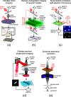
Novel electron imaging methods enabled by light-induced e-beam shaping. (a) Schematic picture of the method used to probe chiral ordering in quantum materials via vortex electron pulses and spectral dichroism following energy postselection. (b) Ramsey-holographic imaging of strongly correlated materials, as obtained by two electron-light interaction points (one above and one below the sample) used to prepare and to read the electron state, respectively, following the interaction with the sample quantum state. (c) Superradiant light emission from excited quantum dots due to the interaction with a phase-modulated light beam, which becomes key in implementing correlative light-electron microscopy with enhanced sensitivity. (d) Schematic diagram of the single-pixel imaging method with momentum space postselection as used for image reconstruction with structured illumination patterns. Adapted from ref . Available under a CC-BY 4.0, Copyright 2023 American Chemical Society. (e) A laser-generated plasma imprints a negative spherical aberration coefficient on the electron transverse profile.
13
13
Classifying the phenomena of free-electron physics in the language of macroscopic-QED (MQED). Subfigures in gray represent effects that are yet to be realized experimentally. (a) Spontaneous emission of photonic quasiparticles. This emission process is forbidden in QED due to the inability to maintain energy−momentum conservation. However, by altering the electromagnetic environment, spontaneous emission is allowed. Depending on the environment, this effect governs various processes, including Cherenkov, Smith−Purcell, transition, and parametric X-ray radiation. The same tree-level diagram in MQED captures all of these effects. First-order emission process of parametric X-ray radiation, demonstrating the quantum recoil correction (middle). Higher-order spontaneous emission and corresponding electron energy spectrum (right). (b) Stimulated absorption and emission of photonic quasiparticles. These processes are described by the sum of all Feynman diagrams where the electron emits and absorbs photonic quasiparticles. Electron energy spectrum after stimulated interaction with classical (coherent state) light, which is the mechanism behind PINEM (middle). Electrons can also interact with nonclassical states of light, as shown with super-Poissonian photon statistics (noisy or chaotic light) (right). The final energy spectrum depends on the quantum statistics of the photons. (c) QED describes self-interactions of free particles due to quantum fluctuations of the vacuum. In bound-electron systems, such self-interactions are responsible for observing the Lamb shift, the anomalous difference in energy between the 2s and 2p orbitals in hydrogen, celebrated as one of the biggest achievements of QED (middle). For free electrons, alteration of the electromagnetic medium (and the explicit breaking of homogeneity) could lead to such self-interactions, which could be measured through diffraction experiments (right). (d) The direct interaction of multiple electrons could generate entanglement between them. Classical energy correlations mediated by Coulomb interactions have recently been observed (middle). , By altering the macroscopic electromagnetic environment and its corresponding dyadic Green function G⃡, these interactions could potentially be enhanced, leading to a strong, controllable generation of entanglement (right). (e) The joint interaction of multiple electrons with a photonic quasiparticle, in combination with postselective measurement of the photons, could lead to the generation of entanglement between the electrons. Interaction with optical photons could lead to the generation of energy entanglement (middle). Interaction with microwave photons in a path-selective manner could lead to the generation of spatial entanglement (right). (f) A similar interaction, with postselective measurement on the electrons instead of the photons, can be used to generate nonclassical light states. By using a single electron and analyzing its postinteraction energy loss, Fock states can be generated, as represented by their Wigner functions (middle). When multiple electrons are involved, more intricate photonic states, such as Schrödinger cat and GKP states, can be created. This is achieved by preshaping the wave functions of the electrons through stimulated emission. The electrons then emit photons, and their energy is measured postinteraction (right). (g) Nonlinear interactions of the electron with the photonic mode can generate quantum light. For slow electrons, the quantum recoil following the emission of a single photon can detune them from the phase-matching condition, facilitating deterministic single-photon emission (middle). When the electron is coupled to a mode where the vector potential ( A ) is perpendicular to the electron’s momentum ( p ), the interaction becomes governed by ponderomotive forces. This interaction, arising from the A 2 term in the minimally coupled Hamiltonian, leads to the emission of photon pairs. As a result, squeezed-vacuum light (SV) is generated (middle).
14
14
Quantum physics and applications at the intersection of electron microscopy and optical spectroscopy. The central elements in this scheme are electrons, light, and matter (lower part), whose characteristics can be described through the joint density matrix ρ e,l,m . Several tools have recently been demonstrated or are still under development, enabling the spatiotemporal shaping of free electrons through interaction with optical fields, the synthesis of entangled electron−photon and electron−matter states, the projection onto subspaces of interest by electron energy and angle postselection, the superradiant emission from multiple electrons, and the measurement of correlations. We envision future applications relying on these tools, specifically in the areas of improved electron microscopy (reduction of e-beam damage, superresolution, supersensitivity, etc.), the retrieval of the quantum dynamics and properties of a specimen, quantum metrology, quantum-enhanced spectromicroscopy, and the generation of quantum light, among other feats. More applications are expected to join this list by leveraging the insights gathered within different areas, as described in this Roadmap. Inset images adapted with permission from refs , , , , , . Copyright 2011 American Chemical Society; Copyright 2022 American Association for Advancement of Science; Copyright 2017 Springer Nature; Copyright 2019 Springer Nature; arXiv; Copyright 2013 American Physical Society.
15
15
Nanophotonics with low-energy electrons in an ultrafast SEM (USEM). (a) Layout of an USEM equipped with a high-resolution electron spectrometer for characterizing electron spectra after inelastic interaction with optical fields. Adapted from ref . Copyright 2022 American Physical Society. (b) Suboptical cycle gating of electrons with two optical pulses at a grating structure. Adapted from ref . Copyright 2017 Springer Nature. (c) Modulation and bunching of electrons induced and detected by the linear interaction with optical near fields in two subsequent periodic nanostructures. , Adapted from ref . Copyright 2019 American Physical Society. (d) SEM images of the structure for complex optical phase-space control (guiding and bunching action) of electrons. Adapted from ref . Copyright 2021 Springer Nature. (e) Picture of a silicon chip hosting five groups of accelerator channels with increasing lengths from 100 to 500 μm. Each group contains eight individual accelerator channels. , (f) SEM image of roughly ten macrocells of the accelerator on a chip (about 200 out of 500 μm of the longest structure shown in (e). Adapted from ref . Copyright 2023 Springer Nature.
16
16
Kapitza−Dirac physics and scattering with low-energy free electrons. (a) Electron scattering at a standing wave formed from two intense laser pulses (left). Shaping of an e-beam inside an SEM with the help of a transversally shaped pulsed laser beam counterpropagating to the e-beam. The optical ponderomotive potential is used to optimize the focusing properties of the e-beam, and more (right). Adapted from ref . Copyright 2022 American Physical Society. (b) Optical traveling waves copropagating with the e-beam inside an SEM are excited to imprint an energy modulation to electrons in a first interaction zone. After propagation, the energy modulation translates into a density modulation, generating an electron attosecond pulse train. ,, Adapted from ref . Copyright 2018 American Physical Society. (c) Quantum-coherent spatiotemporal shaping of electrons by shaped optical fields, including optical vortex beams. , (d) Control of the electron scattering interaction by shaping the electron wave function. −
17
17
Experimental scheme of the proposed Floquet approach. (a) A train of attosecond electron pulses is obtained by interacting photoemitted electrons with the near-field scattering on a sharp tip. (b) The pulse train then excites specific collective modes, namely excitons, in the material. For example, ideal candidates are the excited states of the giant exciton in Cu2O (data taken from ref ). (c) Depending on the pulse train spacing and duration, one can excite different levels of the exciton and, due to the finite momentum of the electrons, the exciton energy dispersion can be directly measured via momentum-resolved EELS.
18
18
Probing exciton excitation, lifetime, coupling, and coherence in 2D semiconductors. (a) 1: SEM image of a probed ZnO MW with a diameter of 2.33 μm. 2: Temperature-dependent CL spectra in the bent region (part II in SEM image). 3: Time-resolved CL for measuring D0XA lifetime, as a function of temperature. Adapted from ref . Copyright 2015 AIP Publishing. (b) Schematic of the developed setup for spectral interferometry. The map shows the interference pattern of the EDPHS and sample radiation at the emitted wavelength of 800 nm in the momentum-delay map, where region R1 corresponds to the existence of mutual coherence, whereas region R2 demonstrates the degradation of the visibility of the interference fringes due to exciton-polariton decoherence. Adapted from ref . Copyright 2023 Springer Nature. (c) STEM image of hBN-encapsulated monolayer MoSe2 suspended on a TEM grid (left), and CL spectra recorded at the positions indicated by P1, P2, P3, and P4 (right). Adapted from ref . Copyright 2023 Royal Society of Chemistry. (d) Sketch of a sample constructed by a WS2 monolayer (orange) encapsulated by two hBN flakes (purple, 20 and 5 nm thickness) on a holey carbon substrate (gray). Localized Trion emission map and EELS−CL spectrum showing Trion excitation. Adapted from ref . Copyright 2021 American Chemical Society. (e) Schematic of a WSe2 thin film supporting waveguided optical modes that are confined in the transverse direction and can strongly interact with excitons. Measured CL spectra for WSe2 thin films with depicted thicknesses. Adapted from ref . Copyright 2022 Wiley. (f) Schematic of a strongly coupled plexciton system composed of an Ag TNP and few-layer WS2. The red, yellow, and blue electron energy-loss spectra are from each corner of the coupled TNP-layer WS2 system, where the STEM image shows corners. Adapted from ref . Copyright 2019 American Chemical Society.
19
19
Local structure−property correlation in plasmonic, catalytic, and quantum nanomaterials probed by e-beams. (a) EELS and electron tomography are used to demonstrate plasmon broadening induced by a single defect in Au nanorods. Modified with permission from ref . Copyright 2020 American Chemical Society. (b) EELS enables spatial and spectral mapping of bright and dark bonding plasmon modes for a gold nanodisk dimer, for which particle distances were modified in situ through a nanoelectromechanical system. Modified with permission from ref . Copyright 2021 Springer Nature. (c) Optically coupled TEM allows imaging and control of light-induced chemical transformations in nanoparticles. Modified with permission from ref . Copyright 2021 American Chemical Society. (d) Operando experiment of CO conversion on Ru catalysts correlating structural modifications of the catalyst to changes in conversion efficiency. Modified from ref . Copyright 2024 American Chemical Society. (e) High-resolution STEM plus EELS determination of the chemical environment of quantum emitters in hBN correlated to their optical emission. Modified from ref . Copyright 2024 American Chemical Society. (f) Integrated CL map of site-selectively generated single-photon emitters in hBN (left). Increasing electron irradiation times led to increasing CL intensities (in photon counts per second). Normalized CL spectra before and after electron irradiation demonstrate the generation of 436 nm emitters (right). Modified from ref . Copyright 2022 American Chemical Society.
20
20
Ptychography with a scanning transmission electron microscope (a) Illustration of the focused-probe electron ptychography method. A convergent beam of high-energy electrons is incident on the specimen. A far-field scattering pattern is collected by a direct electron detector. The electron probe is scanned along the two dimensions of space. (b) Simulated examples of a convergent beam electron diffraction pattern obtained for a collection of scan positions. Recordings are done over a [100]-oriented Au unit cell, with atomic positions indicated in the figure.
21
21
Vision on how key enabling technologies in contrast enhancement/damage reduction and time-resolved electron microscopy could impact the main application sectors.

References

    1. Spence, J. C. H. High-Resolution Electron Microscopy; Oxford University Press: Oxford, 2013.
    1. Dellby N., Lovejoy T., Corbin G., Johnson N., Hayner R., Hoffman M., Hrncrik P., Plotkin-Swing B., Taylor D., Krivanek O.. Ultra-High Energy Resolution EELS. Microsc. Microanal. 2020;26:1804–1805. doi: 10.1017/S1431927620019406. - DOI
    1. Zhu D., Robert A., Henighan T., Lemke H. T., Chollet M., Glownia J. M., Reis D. A., Trigo M.. Phonon Spectroscopy with Sub-MeV Resolution by Femtosecond x-Ray Diffuse Scattering. Phys. Rev. B. 2015;92:054303. doi: 10.1103/PhysRevB.92.054303. - DOI
    1. Egerton, R. F. Electron Energy-Loss Spectroscopy in the Electron Microscope; Plenum Press, 1996.
    1. García de Abajo F. J.. Optical Excitations in Electron Microscopy. Rev. Mod. Phys. 2010;82:209–275. doi: 10.1103/RevModPhys.82.209. - DOI

LinkOut - more resources