. 2025 Oct 8;17(40):56542-56552.
doi: 10.1021/acsami.5c14351. Epub 2025 Sep 29.

Stress-Induced Directed Self-Assembly of Perpendicularly Oriented Block Copolymer Lamellae for Lithographic Density Multiplication

Affiliations

Stress-Induced Directed Self-Assembly of Perpendicularly Oriented Block Copolymer Lamellae for Lithographic Density Multiplication

Aum Sagar Panda et al. ACS Appl Mater Interfaces. .

Abstract

This work demonstrates a stress-induced directed self-assembly (DSA) approach to produce unidirectionally oriented perpendicular lamellae in block copolymer (BCP) thin films, achieving a smaller line width and a higher aspect-ratio for pattern transfer with lithographic density multiplication. A free-standing polystyrene-block-polydimethylsiloxane (PS-b-PDMS) thin film on a transmission electron microscopy (TEM) grid is thermally annealed under high vacuum inside an in situ, temperature-resolved TEM instrument. The high vacuum reduces the surface tension discrepancy between PS and PDMS at high temperatures, creating neutral surfaces at both top and bottom sides of the thin film and facilitating the formation of film-spanning perpendicular lamellae via self-alignment during thermal annealing. Finite element analysis reveals that the x-directional stress is concentrated at the grid edge, inducing the formation of unidirectionally oriented perpendicular lamellae, as evidenced by an in situ, time-resolved TEM observation. This edge-parallel alignment arises from a tensile stress gradient along the edge-normal direction, which favors lamellae aligned parallel to the edge to minimize elastic mismatch between PS and PDMS during self-assembly. For nanopatterning, the free-standing thin film is transferred onto substrates with e-beam-defined trenches followed by thermal annealing in a homemade vacuum oven. The BCP film gradually flows into the trenches during which the stress guides the formation of unidirectionally oriented perpendicular lamellae. Subsequently, well-defined SiO2 line patterns can be formed within the trenches after O2 reactive ion etching. This facile method enables controlled orientation of a free-standing BCP thin film by integrating vacuum-driven perpendicular orientation and stress-induced DSA, providing appealing potential for fabrication of highly ordered line patterns in advanced lithographic applications.

Keywords: block copolymer; controlled orientation; directed self-assembly; finite element analysis; vacuum.


Figures
1
1
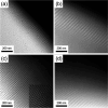
Stress-induced unidirectionally oriented perpendicular lamellae. Time series of in situ, temperature-resolved TEM imaging of a free-standing PS-b-PDMS thin film after thermal annealing at 300 °C for (a) 5 min; (b) 30 min; (c) 60 min (the inset shows the defect annihilation process); (d) 120 min.
2
2
Stress analysis of PS-b-PDMS free-standing thin film using FEA analysis. (a) Out-of-plane (Z-direction) displacement profile showing maximum deformation at the center of the suspended region. (b) X-directional stress distribution of the free-standing PS-b-PDMS thin film on the topographically patterned SiO2 substrate, with tensile stress localized along the edges of the SiO2 mesa (trench widths = 2000 nm). (c) Schematic illustration of stress concentration near the copper bars of a TEM grid, arising from tension induced by film bending under gravity. Nucleation of stress-induced unidirectionally perpendicular lamellae is initiated from the stress concentrated region. The inset shows the preferred orientation of lamellae.
3
3
Schematic illustration of the film transfer process and stress-induced DSA on a topographically patterned substrate. (a) A PS-b-PDMS thin film on a Si wafer with a native SiO2 layer; (b) a floating thin film on water after HF etching of the SiO2 layer; (c) transferring the floating thin film to a topographically patterned wafer with e-beam-defined trenches; (d) a free-standing PS-b-PDMS thin film on a topographically patterned wafer with e-beam-defined trenches; (e) the initial film conditions under high-vacuum thermal annealing during which the PS-b-PDMS thin film flows into the trench; (f) formation of unidirectional perpendicular lamellae in the free-standing thin film; (g) the final film conditions with unidirectionally oriented perpendicular lamellae within the topographic trenches.
4
4
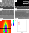
Cross-sectional FE-SEM images of (a) a topographically patterned wafer with trenches; (b) a free-standing PS-b-PDMS thin film on the topographic trench; (c) PS-b-PDMS thin film conformally filling the topographic trench after thermal annealing under vacuum. The inset shows the unidirectionally oriented perpendicular lamellae within the trench after O2 RIE; (d) a top-view FE-SEM image of unidirectionally oriented perpendicular lamellae after O2 RIE; (e) a 2D GISAXS pattern of unidirectionally oriented perpendicular lamellae after O2 RIE; (f) the 1D integral profile of GISAXS.
5
5
FE-SEM images of well-aligned SiO2 line patterns from the free-standing PS-b-PDMS thin film on a topographic pattern with trench widths of (a) 300 nm; (b) 500 nm; (c) 750 nm; (d) 1000 nm. The thin films were thermally annealed under vacuum (10–4 Pa) at 300 °C for 2 h followed by O2 RIE (the scale bars are 250 nm). The lamellar nanostructures exhibit unidirectional orientation with increasing domain density as the trench width increases, corresponding to density multiplication factors of approximately (a) 18×, (b) 34×, (c) 50×, and (d) 66×, respectively, relative to the trench pitch length defined by e-beam lithography. (e–h) Orientational color analysis of well-aligned SiO2 line patterns from the free-standing PS-b-PDMS thin film on a topographic pattern with trench widths of (e) 300 nm; (f) 500 nm; (g) 750 nm; (h) 1000 nm. The scale bars are 250 nm. The inset shows the orientational color bar.

References

    1. Bates F. S., Fredrickson G. H.. Block Copolymer Thermodynamics: Theory and Experiment. Annu. Rev. Phys. Chem. 1990;41:525–557. doi: 10.1146/annurev.pc.41.100190.002521. - DOI - PubMed
    1. Bates F. S., Fredrickson G. H.. Block Copolymers Designer Soft Materials. Phys. Today. 1999;52:32–38. doi: 10.1063/1.882522. - DOI
    1. Park C., Yoon J., Thomas E. L.. Enabling Nanotechnology with Self Assembled Block Copolymer Patterns. Polymer. 2003;44:6725–6760. doi: 10.1016/j.polymer.2003.08.011. - DOI
    1. Hawker C. J., Russell T. P.. Block Copolymer Lithography: Merging “Bottom-Up” with “Top-Down” Processes. MRS Bull. 2005;30:952–966. doi: 10.1557/mrs2005.249. - DOI
    1. Segalman R. A.. Patterning with Block Copolymer Thin Films. Mater. Sci. Eng., R. 2005;48:191–226. doi: 10.1016/j.mser.2004.12.003. - DOI

LinkOut - more resources