Review
. 2025 Oct 9;14(1):359.
doi: 10.1038/s41377-025-01939-2.

Peculiarities of room temperature organic photodetectors

Affiliations
Review

Peculiarities of room temperature organic photodetectors

Antoni Rogalski et al. Light Sci Appl. .

Abstract

Organic semiconductors (OSCs) have been considered as projecting family of optoelectronic materials broadly investigated for more than 40 years due to capability to tune properties by adjusting chemical structure and simple processing. The OSCs performance has been substantially increased, due to the fast development in design and synthesis. The spectral response of OSCs was extended from ultraviolet (UV) to near infrared (NIR) wavelength region. There are papers reporting detectivity (D*) higher than the physical limits set by signal fluctuations and background radiation. This paper attempts to explain the organic photodetectors' peculiarities when confronted with typical devices dominating the commercial market. To achieve this goal, the paper first briefly describes OSC deposition techniques, diametrically opposed to those used for standard semiconductors. This was followed by a more detailed discussion of basic physical properties, contributing to the photodetectors' performance including absorption coefficient, conduction mechanism, charge generation and charge transport. These effects are very different from those found in inorganic semiconductors (ISCs). The second part of the paper describes the main modes of OSC based photodetectors [photoconductors, photodiodes and field effect transistor photodetectors (FET)] with emphasis on their special features that distinguish them from standard photodetectors. Final part of the paper shows current state-of-the-art of various types/structures of photodetectors and routes for further improvement. The upper detection limit for OSC photodiodes has been shown to be comparable to that for ISC photodiodes with nearly three orders of magnitude variation. The D* overestimates (especially organic based FET phototransistors) were explained.


Conflict of interest statement

Conflict of interest: The authors declare no competing interests.

Figures

Fig. 1
Fig. 1. Carbon (sixth element in the periodic table, electron configuration 1s22s22p2) as the main building block of OSCs.
a The combination of the sp2 (hybridized) and 2pz (unhybridized) orbitals to create the σ-/π-bonds in a carbon-carbon double bond. b Origin of OSC’s band structures - extension of molecular orbitals to long conjugated oligomers and polymers (Reproduced with permission for ref. © 2020 Griffith, Cottam, Stamenkovic, Posar and Petasecca). CB-conduction band, VB-valence band
Fig. 2
Fig. 2
Example of donor molecules for OSC photodetectors for UV to the short wavelength infrared (SWIR)
Fig. 3
Fig. 3. The OSCs doping fundamental principles.
a Pristine. b p-doped. c n-doped OSCs. The energy levels (occupied bands are shaded, and empty bands are clear) and corresponding density of states (DOS). U gap is created between the SOMO and SOMO* bands of the doped OSCs. The doped OSC work function (WF) is a convolution of the shallowest occupied and deepest empty states. IE-ionization energy, EA-electron affinity (Reproduced with permission for ref. © 2023 Tang, Hou, Leong. Published by American Chemical Society)
Fig. 4
Fig. 4. Electron mobilities at room temperature.
a Comparison of mobilities of various material systems with standard semiconductors used in the photodetectors’ fabrication [transition metal dichalcogenides (TMDs), colloidal quantum dots (CQDs), black phosphorus (bP)]. b The field dependent mobility evolution in organic FET transistors (Reproduced with permission for ref. © American Chemical Society)
Fig. 5
Fig. 5. Absorption coefficient of organic molecules.
a Non-fullerene acceptors FBR 27 (red) and IDTBR28 (cyan), donor polymer PTB7-Th29,30 (blue), and their blends (ratio 1:2) (purple, light blue) extracted from UV − VIS measurements (Reproduced with permission for ref. © 2018 Krückemeier, Kaienburg, Flohre, Bittkau, Zonno, Krogmeier, Kirchartz). b DPPTTT, IDTBT, PSeDPPBT and PBTTT films, measured by photothermal deflection spectroscopy (Reproduced with permission for ref. © Nature)
Fig. 6
Fig. 6
Absorption coefficient at room temperature as a function of the band gap energy for selected materials (Reproduced with permission for ref. © 2023 Rogalski, Kopytko, Hu, Martyniuk. Licensee MDPI, Basel, Switzerland)
Fig. 7
Fig. 7
Carrier lifetimes for various material systems
Fig. 8
Fig. 8
The carriers’ generation mechanisms in OSCs: photoexcitation, exciton dissociation, charge carrier transport, and recombination and extraction processes required to extract free charge
Fig. 9
Fig. 9
Operating mechanisms for general type o OSC photodetector. The basic processes occurring in the detector are explained in the description of Fig. 8
Fig. 10
Fig. 10
The room temperature D* for OSC based detectors compared with typical devices (Si, AlGaN, Ge, InGaAs PDs and PMTs) for λ = 0.2–2 μm. The utmost BLIP and SFL are also presented. PD-photodiode, PMT-photomultiplier tube, FET-field effect transistor, PV-photovoltaic detector. The OSC photodetectors’ D* marked in magenta are overestimated
Fig. 11
Fig. 11
Pros and cons of the PC, PV, and PT detectors
Fig. 12
Fig. 12. Operation modes of OFET device.
a Ideal output source-drain current characteristics for different gate voltages. b The linear mode. c At pinch-off. d The saturation mode
Fig. 13
Fig. 13. The performance of the photodiodes, photoconductors and photo-FETs.
a Photocurrent/responsivity versus radiation power. b Gain versus frequency
Fig. 14
Fig. 14
Schematic structures of OPDs: the standard and inverted structures with the BHJ and PHJ for the active/absorption layer (Reproduced with permission for ref. © 2022 Shan, Hou, Yin, Guo)
Fig. 15
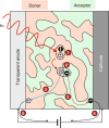
Fig. 15. The carrier injection mechanism in OSCs photodiodes.
a BHJ with percolating networks. b BHJ with blocking layers. c Quasi-planar heterojunction (q-PHJ) with vertical phase segregation (Reproduced with permission for ref. © 2022 Shan, Hou, Yin, Guo)
Fig. 16
Fig. 16. The structure of OSCs based photodetector ITO/ZnO/PDPP3T:PC71BM/A with a broad response and high gain.
a Device structure of the broadband photodetector. b Energy diagram for constituent materials. c EQE spectra measured under selected voltages for UV (Reproduced with permission for ref. © 2016 WILEY-VCH Verlag GmbH & Co. KGaA, Weinheim)
Fig. 17
Fig. 17. The mid-gap trap states contribution to the OSC based photodiodes performance.
a Dark current densities curves (square, triangles and circles based on ref. ; diamonds from the selected published papers). b Extracted dark saturation current density versus energy gap (the red solid line corresponds to a trend line Jd=J0expqV/2kT with factor J0 = 2 × 10³ A/cm2, a shaded area corresponds an upper level J0 = 2 × 10⁵ A/cm2 and lower level Jd = 20 A/cm2). c The trends for band-to-band (activation energy Ea = Eg) and mid-gap transitions (Ea = Eg /2) are shown by the blue dashed and red solid lines. d The estimated upper limit of detectivity − simulated based on the red solid line in Fig. b, the red shaded region corresponds the shaded area in Fig. b (Reproduced with permission for ref. © 2023 Sandberg, Kaiser, Zeiske, Zarrabi, Gielen, Wouter Maes, Vandewal, Meredith, Armin)
Fig. 18
Fig. 18. Photodiodes with the low-bandgap PDPP3T polymer blended with PC71BM.
a Device structure layout. b Energy band levels diagram for OSCs photodiode fabrication. c J-V characteristics measured in dark and under 850 nm light conditions (2.7 μW). d Calculated detectivity for poly-TPD or PEDOT:PSS as the anode interlayer under −0.5 V bias (Reproduced with permission for ref. © Wiley)
Fig. 19
Fig. 19
Normalized EQE for OSCs narrow-photo-absorbing based photodiodes versus wavelength. 1(Pyrl):C60 and Cy7-T:C60 are PHJs (2:PC61BM is a BHJ blend). PSQ and ISQ are single-component photo-absorbing materials with D/A/D chemical structure and U3 is also single component device (Reproduced with permission for ref. © The Royal Society of Chemistry 2022)
Fig. 20
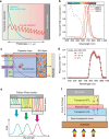
Fig. 20. Operation principle of narrow-band OPDs structures.
a The schematic structure of CCN photodiode. b Normalized EQE for selected absorber thicknesses (Reproduced with permission for ref. © Nature). c Self-filtering photodiode operating mechanism. d Responsivity spectra measured for the filter-free visible-blind NIR OPD operated under selected voltages: 0, -0.4 and -1 V (Reproduced with permission for ref. © Wiley). e Fabry-Perot cavity (the length of optical spacer determines the resonance wavelength) operating fundamentals. f Fabry-Perot cavity in a photodetector with partially transparent bottom mirror (electrode)
Fig. 21
Fig. 21. Energy band profiles and operating mechanisms for photomultiplication effect in OPDs.
a Ultra-low concentration of one component (example of acceptor). b Interfacial blocking layer (HBL) (Reproduced with permission for ref. © 2022 Shan, Hou, Yin, Guo, corrected publication 2022)
Fig. 22
Fig. 22. Photomultiplication-type BDP-OMe:C60 photodetector.
a Device structure. b Device band energy diagram. c EQE for selected donor concentration under − 10 V. d Comparison of current responsivity and detectivity versus reverse voltage for devices: PM-PD, p-i-n PD and n-i-p PD (Reproduced with permission for ref. © 2022 Xing, Kublitski, Hänisch, Winkler, Li, Kleemann, Benduhn, Leo. Advanced Science published by Wiley-VCH GmbH)
Fig. 23
Fig. 23. The OSCs phototransistor.
a Design of the PQT-12/F4-TCNQ phototransistor, on right: molecules structure of F4-TCNQ and PQT-12. b Absorption spectra of the F4-TCNQ film, PQT-12 film, and PQT-12/F4-TCNQ film. c The current responsivity and detectivity versus light power for λ = 2000 nm and VG = ‒20 V (black dots - responsivity, red dots - detectivity). d Current responsivity and response time versus wavelength for VG = ‒20 V (Reproduced with permission for ref. © Wiley)
Fig. 24
Fig. 24. Characteristics of organic FET phototransistors.
a EQE of naphthalene diimide-phenylmethyl (NDI-PM) nanorod (NR)-based phototransistor for UV light powers 100 and 1 μW cm-2. b Detectivity versus current responsivity for VIS-blind UV photodetectors presented in refs. The measured results within the grey box are overestimated
Fig. 25
Fig. 25
Challenges for emerging OPDs

References

    1. Peumans, P., Yakimov, A. & Forrest, S. R. Small molecular weight organic thin-film photodetectors and solar cells. J. Appl. Phys.93, 3693–3723 (2003).
    1. Forrest, S. R. The path to ubiquitous and low-cost organic electronic appliances on plastic. Nature428, 911–918 (2004). - PubMed
    1. Shaheen, S. E., Ginley, D. S. & Jabbour, G. E. Organic based photovoltaics: toward low-cost power generation. MRS Bull.30, 10–19 (2005).
    1. Scott, J. C. & Bozano, L. D. Nonvolatile memory elements based on organic materials. Adv. Mater.19, 1452–1463 (2007).
    1. Xue, J. G. Perspectives on organic photovoltaics. Polymer Rev.50, 411–419 (2010).

LinkOut - more resources