. 2025 Oct 30;16(1):9590.
doi: 10.1038/s41467-025-62863-y.

Kinetically-controlled intermediate-direct-pinning for homogeneous energy landscapes in quasi-two-dimensional perovskites for efficient and narrow blue emission

Affiliations

Kinetically-controlled intermediate-direct-pinning for homogeneous energy landscapes in quasi-two-dimensional perovskites for efficient and narrow blue emission

Joo Sung Kim et al. Nat Commun. .

Abstract

Quasi-two-dimensional perovskite structures hold great potential as active layers in blue perovskite light-emitting diodes. However, they face challenges of limited emission efficiency and broadened spectra due to phase inhomogeneity. Here, we report an intermediate-direct-pinning method to develop a uniform-phase quasi-two-dimensional structure with a homogeneous energy landscape. By forming a strong cation-π interaction complex, we stabilize a metastable intermediate phase with retarded crystallization toward low-n phases (n ≤ 3), followed by a direct pinning process favouring crystallization of medium-n phases (n = 4 and 5) without further broadening. Additionally, introducing a surface-anchoring ligand during the pinning process effectively suppresses non-radiative recombination. The resultant structure shows efficient sky-blue emission and narrow linewidth (108 meV). Devices fabricated with this structure reach a maximum external quantum efficiency of 22.5% at 489 nm, which is scalable to large-area (pixel size: 900 mm2) and passive matrix devices (30 × 10 arrays, active area = 200 μm × 600 μm). These findings highlight the potential of perovskite light-emitting diodes for full-colour displays.


Conflict of interest statement

Competing interests: The authors declare no competing interests.

Figures

Fig. 1
Fig. 1. Anchoring-assisted intermediate direct pinning for quasi-2D perovskites.
a Schematic reaction coordinate of the intermediate direct pinning (IDP) process of quasi-2D perovskites. b, c Grazing-incident x-ray diffraction pattern corresponding 1D XRD profile of pristine (b) and A-IDP (c) perovskite thin films. d X-ray diffraction spectra of n = 1 PEA2PbBr4 perovskites without and with CCA additives as molecular anchor. e Relative content of carbon and nitrogen to lead in perovskite films determined from XPS. f Normalized UV-vis absorption and PLE spectra of pristine and A-IDP perovskite films. g Steady-state PL spectra of perovskite films.
Fig. 2
Fig. 2. Intermediate-assisted bright blue-emitting quasi-2D perovskites.
a, b NOESY 2D 1H NMR of perovskite precursor solution without MDACl2 (a) and with MDACl2 (b). c Schematic figure on the mechanism of cation-π intermediate complex formation. d Schematic illustration of crystallization process with (upper panel) and without (bottom panel) MDACl2 in sequence of solution state, film state after spin-coating, IDP process, and thermal annealing process, each from left to right. Inset of the scheme after spin-coating: Picture of thin films with different time after spin-coating. Scale bar, 1 cm. e Steady-state PL spectra of quasi-2D perovskite thin films with different amount of MDACl2 substitution. f Steady-state PL intensity and FWHM of perovskite films different amount of MDACl2 substitution and A-IDP process. g PLQY and FWHM of perovskite films different amount of MDACl2 substitution and with or without A-IDP process.
Fig. 3
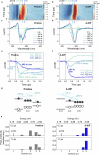
Fig. 3. Femtosecond TA spectra of pristine and A-IDP perovskite films.
a, b 2D contour plot and c, d early-time spectra of pristine (a, c) and A-IDP (b, d) films. e, f TA kinetic traces of pristine (e) and A-IDP (f) perovskite films probed at 450 nm, 470 nm, 488 nm, each corresponding to domains of n = 3,4,5, respectively. g Schematic description of the charge carrier funnelling occurring in pristine and A-IDP films. The DOS were qualitatively estimated from the initial carrier population distribution (TA spectra at t = 0.2 ps). h Carrier population distribution of pristine and A-IDP films presented by the weighted average peak area of TA spectra at delay times 0.2 ps (upper panels) and 1 ps (lower panels).
Fig. 4
Fig. 4. EL characteristics of blue PeLEDs.
a schematic energy diagram of PeLEDs. b luminance and current density vs voltage, c EQE vs current density (inset: operating PeLEDs without (left) and with (right) hemispherical lens, scale bar: 1 cm), d normalized EL spectra, e EQE histogram of PeLEDs. f Characteristics of reported blue PeLEDs with peak emission wavelength <495 nm based on maximum EQE and EL linewidth. Summarized in Supplementary Table 3. g Photograph of operating large-area PeLEDs (pixel size: 900 mm2). Scale bar: 1 cm. h Schematic structure and picture of operating 30 × 10 passive-matrix PeLEDs (active area = 200 μm × 600 μm). Scale bar: 1 mm.

References

    1. Cho, H. et al. Overcoming the electroluminescence efficiency limitations of perovskite light-emitting diodes. Science. 350, 1222–1225 (2015). - PubMed
    1. Han, T.-H. et al. A roadmap for the commercialization of perovskite light emitters. Nat. Rev. Mater.7, 757–777 (2022).
    1. Ma, D. et al. Distribution control enables efficient, reduced-dimensional perovskite LEDs. Nature599, 594–598 (2021). - PubMed
    1. Kim, Y.-H. et al. Comprehensive defect suppression in perovskite nanocrystals for high-efficiency light-emitting diodes. Nat. Photon.15, 148–155 (2021).
    1. Kim, J. S. et al. Ultra-bright, efficient and stable perovskite light-emitting diodes. Nature611, 688–694 (2022). - PubMed

LinkOut - more resources