Tunable Semiconducting Behavior and Linear-Nonlinear Optical Properties of Ag-Sn Dual-Doped Nanocrystalline CdO Thin Films for Optoelectronics
- PMID: 41179171
- PMCID: PMC12573159
- DOI: 10.1021/acsomega.5c03249
Tunable Semiconducting Behavior and Linear-Nonlinear Optical Properties of Ag-Sn Dual-Doped Nanocrystalline CdO Thin Films for Optoelectronics
Abstract
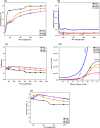
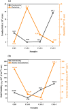
Semiconductor-based thin films have a great impact on determining the anticipated optoelectronic device construction and the advancement of cutting-edge applications. Herein, Ag and Sn dual-doped nanocrystalline transparent conducting CdO thin films were prepared on glass substrates using a cost-effective spray coating method, and their structural, morphological, optical, and semiconducting behaviors were investigated. The successful incorporation of Ag and Sn resulted in the polycrystalline nature of the deposited films without the additional peaks, as verified by X-ray diffraction (XRD) analysis. The XRD report also revealed the enhanced crystallinity (65%) at the higher doping level (3 wt % Ag and Sn-doped CdO film). All the deposited CdO films exhibited homogeneous, spherical, or round-shaped grains, with agglomeration revealed by scanning electron microscopy analysis. UV-visible spectroscopy was utilized to determine the linear and nonlinear optical properties of the deposited CdO thin films, and a reduction in the band gap from 3.891 to 3.772 eV was observed. A significant enhancement in the first- and third-order nonlinear susceptibility and nonlinear refractive index of the doped CdO films was also observed with increasing doping concentration. Hall effect data were collected at room temperature to investigate the electrical properties of all of the CdO films. The charge carrier concentration of CdO thin films was increased from 142.08 × 10¹⁸ to 169.10 × 1018 cm-3, and the highest conductivity was found to be 192 s/cm on doping 3 wt % Ag-Sn. All the CdO thin films exhibited n-type conductivity, while an incredible n-type to p-type charge carrier transition was noticed at a higher doping level (3 wt % Ag-Sn). The findings of the current work are expected to advance the synthesis of semiconductor thin films through cost-effective spray coating methods for optoelectronic device applications.
© 2025 The Authors. Published by American Chemical Society.
Figures


References
-
- Hall R. N., Fenner G. E., Kingsley J. D., Soltys T. J., Carlson R. O.. Coherent Light Emission From GaAs Junctions. Phys. Rev. Lett. 1962;9:366–368. doi: 10.1103/PhysRevLett.9.366. - DOI
-
- Pedersen H., Elliott S. D.. Studying chemical vapor deposition processes with theoretical chemistry. Theor. Chem. Acc. 2014;133:1476. doi: 10.1007/s00214-014-1476-7. - DOI
-
- Afre R. A., Sharma N., Sharon M., Sharon M.. Transparent Conducting Oxide Films for Various Applications: A Review. REVIEWS ON ADVANCED MATERIALS SCIENCE. 2018;53:79–89. doi: 10.1515/rams-2018-0006. - DOI
-
- Chang H. J., Chen W. F., Huang K. M., Ho C. L., Wu M. C.. Deposition of Transparent Indium Molybdenum Oxide Thin Films and the Application for Organic Solar Cells. Jpn. J. Appl. Phys. 2012;51:02BK02. doi: 10.1143/JJAP.51.02BK02. - DOI
LinkOut - more resources
Full Text Sources
Miscellaneous
