. 2025 Nov 5;25(21):6772.
doi: 10.3390/s25216772.

320 × 240 SPAD Direct Time-of-Flight Image Sensor and Camera Based on In-Pixel Correlation and Switched-Capacitor Averaging

Affiliations

320 × 240 SPAD Direct Time-of-Flight Image Sensor and Camera Based on In-Pixel Correlation and Switched-Capacitor Averaging

Maarten Kuijk et al. Sensors (Basel). .

Abstract

Correlation-Assisted Direct Time-of-Flight (CA-dToF) is demonstrated for the first time on a large 320 × 240-pixel SPAD array sensor that includes on-chip high-speed timing support circuitry. SPAD events are processed in-pixel, avoiding data communication over the array and/or storage bottlenecks. This is accomplished by sampling two orthogonal triangle waves that are synchronized with short light pulses illuminating the scene. Using small switched-capacitor circuits, exponential moving averaging (EMA) is applied to the sampled voltages, delivering two analog voltages (VQ2, VI2). These contain the phase delay, or the time of flight between the light pulse and photon's time of arrival (ToA). Uncorrelated ambient photons and dark counts are averaged out, leaving only their associated shot noise impacting the phase precision. The QVGA camera allows for capturing depth-sense images with sub-cm precision over a 6 m range of detection, even with a small PDE of 0.7% at an 850 nm wavelength.

Keywords: 3D-ToF; CA-dToF; LIDAR; SPAD; depth sensing; exponential moving average; switched capacitors.


Conflict of interest statement

The authors declare no conflict of interest.

Figures

Figure 1
Figure 1
An example of a noisy data stream on which the simple moving average (SMA) and the exponential moving average (EMA) are applied with navg = 30. A similar averaging is obtained.
Figure 2
Figure 2
This circuit implements the EMA: the capacitor Cs charges to Vk; when a pulse is applied to Vnext, the switch toggles to the right, during which Cs and Cint become shorted. A new voltage based on charge sharing is established, resulting in the updated VEMA.
Figure 3
Figure 3
The practical EMA implementation consists of generating non-overlapping clocks (f1 and f2) in response to an edge transition from Vnext, driving the gates of two NMOS transistors (left); the parasitic capacitance of the substrate diffusion diode between the two transistors forms Cs (center); the non-linear behavior of Cs and Cint form spice simulation and are shown on the right.
Figure 4
Figure 4
By periodically toggling the switch, a low-pass filter is constructed, with −3 dB corner frequency settable by the toggling frequency fs.
Figure 5
Figure 5
An analog counter based on a switched-capacitor principle, useful for counting events like incident photons. When zooming-in, the step-like behavior becomes visible (in green).
Figure 6
Figure 6
The correlation functions TCOS and TSIN (left) and the schematic (right) of the two-stage averaging system for correlating the incident ToAs of photons with these functions.
Figure 7
Figure 7
Statistical simulation of a frame of 125 k cycles showing the averaging of the sampled TCOS and TSIN after the first and after the second averaging stages (left). On the right, the distance is calculated based on Equations (6) and (7) and the indicated toggling frequency fs is reduced by a factor of 10 after 40% of the frame.
Figure 8
Figure 8
The pixel circuit has a non-overlapping clock generator, a photon counter, and two-stage averaging for the sampled triangular TSIN and TCOS signals.
Figure 9
Figure 9
The camera is controlled by a PC over USB3 (right). An FX3 microcontroller (Infineon) provides communication with the PC through direct memory access with the image sensor chip. Left: experimental camera setup and measured triangular waveforms generated on-chip.
Figure 10
Figure 10
Timing diagram containing (a) subframes for gray value and 3D acquisition; (b) exposure and readout subframes, and (c) demodulation signals for 25 and 100 MHz subframes with the laser pulse position depending on the phase of the frame.
Figure 11
Figure 11
Demodulation using (0°, 180°) phases at 25 MHz: Gray, Q2, I2, and 3D images. Shown right are cross-sections from the image’s row 124, giving more quantitative results, including measured and modeled depth STDV. Color scale is present in the depth-graph (upper right). Ambient is 1 klux at the whiteboard (b) and 2 klux at the box (e).
Figure 12
Figure 12
Demodulation at (0°, 180°) phases at 25 MHz and (0°, 180°, 90°, 270°) phases at 100 MHz. Ambient situation is the same as the previous experiments. Color scale is present in the depth-graph (center).
Figure 13
Figure 13
Demodulation at (0°, 180°) phases at 25 MHz and (0°, 180°, 90°, 270°) phases at 100 MHz, including a spatial filter in post-processing. Same ambient situation as in Figure 5. Fixed pixel noise (in cm) is demonstrated on the “flat” surface of the box (e). Color scale is present in the depth-graph (center).
Figure 14
Figure 14
Accuracy of a pixel in the center of the image. The laser is cycled over the full 360° phase range in 64 steps. The level of cyclic error is then obtained by plotting the accuracy error, being the difference between the calculated distance (derived from Q2 and I2) and the ground truth.
Figure 15
Figure 15
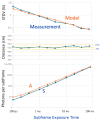
Experiment showing variable exposure time for depth sensing, from 100 us to 80 ms. The measured average A and S (bottom) are indicated, as well as the measured and modeled STDV, based on A and S (top). Depth variations remain within +/− 1% (middle).
Figure 16
Figure 16
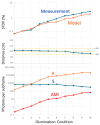
Experiment with an increasing amount of ambient light from A = 251 to 20,066 photons per subframe (bottom). Indicated are A, S, and ASR (bottom). The measured distance (center) and the modeled and measured STDV (top).
Figure 17
Figure 17
Estimated distance versus ground truth (top). Error on the distance (center); STDV of the estimated distance (bottom).

References

    1. Bastos D., Monteiro P.P., Oliveira A.S.R., Drummond M.V. An Overview of LiDAR Requirements and Techniques for Autonomous Driving; Proceedings of the 2021 Telecoms Conference (ConfTELE); Leiria, Portugal. 11–12 February 2021; pp. 1–6.
    1. ALi Y., Ibanez-Guzman J. Lidar for Autonomous Driving: The Principles, Challenges, and Trends for Automotive Lidar and Perception Systems. IEEE Signal Process. Mag. 2020;37:50–61. doi: 10.1109/msp.2020.2973615. - DOI
    1. Horaud R., Hansard M., Evangelidis G., Ménier C. An overview of depth cameras and range scanners based on time-of-flight technologies. Mach. Vis. Appl. 2016;27:1005–1020. doi: 10.1007/s00138-016-0784-4. - DOI
    1. Bamji C., Godbaz J., Oh M., Mehta S., Payne A., Ortiz S., Nagaraja S., Perry T., Thompson B. A Review of Indirect Time-of-Flight Technologies. IEEE Trans. Electron Devices. 2022;69:2779–2793. doi: 10.1109/TED.2022.3145762. - DOI
    1. Kawahito S., Yasutomi K., Mars K. Hybrid Time-of-Flight Image Sensors for Middle-Range Outdoor Applications. IEEE Open J. Solid-State Circuits Soc. 2022;2:38–49. doi: 10.1109/OJSSCS.2021.3133224. - DOI

LinkOut - more resources