. 2025 Nov 28;16(1):10723.
doi: 10.1038/s41467-025-65750-8.

Improving interfacial thermal conductivity by constructing covalent bond between Ga₂O₃ and SiC

Affiliations

Improving interfacial thermal conductivity by constructing covalent bond between Ga₂O₃ and SiC

Yi Shen et al. Nat Commun. .

Abstract

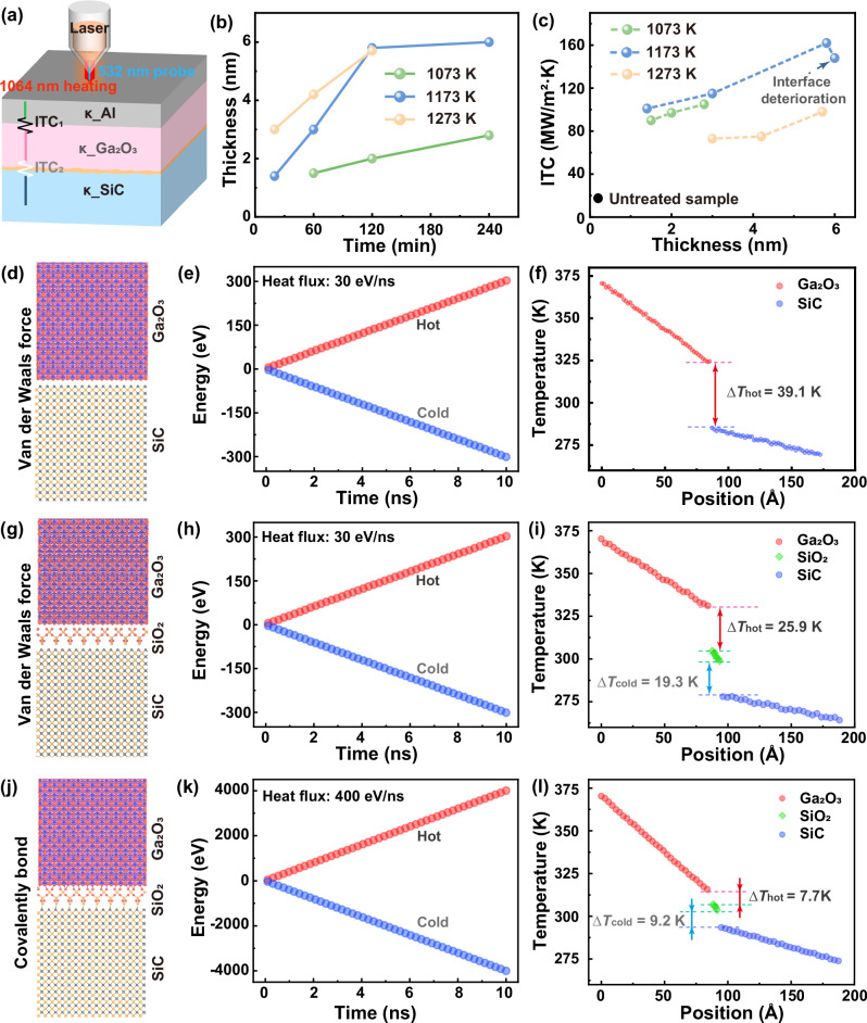
Gallium oxide (Ga₂O₃) is emerging as a promising semiconductor for next-generation power and radio-frequency electronics due to its ultra-wide bandgap and high breakdown field. Yet, its intrinsic thermal conductivity is extremely low, which causes severe self-heating and limits reliable device operation. A common approach to overcome this challenge is to integrate Ga₂O₃ with substrates of high thermal conductivity such as silicon carbide (SiC). However, weak bonding across the heterojunction interface creates large thermal resistance, preventing efficient heat removal. Here we show that constructing strong covalent bonds between Ga₂O₃ and SiC through an engineered interlayer enables both structural compatibility and efficient phonon transport. This bonding strategy increases the interface thermal conductivity to 162 MW/m²·K, the highest value reported for Ga₂O₃ heterostructures. Infrared thermography confirms that the bonded devices exhibit a temperature reduction of up to 29 °C under high power densities, demonstrating significant mitigation of self-heating. These findings establish a practical route for enhancing thermal management in Ga₂O₃ electronics and highlight the importance of interfacial bonding design. Beyond Ga₂O₃, this approach may be extended to other wide-bandgap semiconductors where thermal bottlenecks constrain device performance.


Conflict of interest statement

Competing interests: The authors declare no competing interests.

Figures

Fig. 1
Fig. 1. TEM images of Ga₂O₃/SiC and Ga₂O₃/SiO₂/SiC heterojunctions before and after annealing.
a Schematic of the fabrication process. b Cross-sectional TEM image and corresponding EDS maps of the untreated sample. c EDS line scans of the cross-section. d HRTEM micrograph of Ga₂O₃/SiC heterojunction interface and SAED pattern (e) Cross-sectional TEM image and corresponding EDS maps of the sample annealed for 120 min at 1173 K. f EDS line scans of the cross-section. g HRTEM micrograph of Ga₂O₃/SiO2/SiC heterojunction interface and SAED pattern.
Fig. 2
Fig. 2. Structural characterization of as-deposited and annealed samples by XRD and XRR analyses.
a XRD patterns and (b) Measured and fitted XRR curves of the as-deposited and annealed samples. ce The extracted XRR data for the corresponding layers and the error bars represent standard deviation.
Fig. 3
Fig. 3. Depth-resolved XPS analysis and structural evolution of Ga₂O₃/SiC heterojunctions before and after annealing.
a Depth-profiled XPS spectral maps corresponding to Si 2 s and O 1 s core-level features across the Ga₂O₃/SiC heterojunction in the untreated sample. b The corresponding Si 2 s and O 1 s XPS peaks at different etching depths. c Depth-profiled XPS spectral maps corresponding to Si 2 s and O 1 s core-level features across the Ga₂O₃/SiC heterojunction in the sample annealed for 120 min. d The corresponding Si 2 s and O 1 s XPS peaks at different etching depths. e Schematic crystal structures of β-Ga₂O₃ and amorphous Ga₂O₃ after high-temperature thermalization. f Radial distribution function of amorphous Ga₂O₃. g Heterogeneous interface of Ga₂O₃ and 4H-SiC before and after the reaction. h Si-O bond ratios vary with reaction time.
Fig. 4
Fig. 4. The TDTR experimental and MD simulation analysis of interfacial thermal transport across Ga₂O₃/SiC and Ga₂O₃/SiO₂/SiC heterojunctions with different bonding configurations.
a Schematic diagram of the sample structure and the TDTR experiment. b The thickness of SiO2 layer as a function of time at different temperatures. c The ITC values established via the TDTR measurements at different thickness of SiO2 layer. d, g, j Structural modeling for molecular dynamics calculations at the Ga₂O₃/SiC interface bonded by (d) VdW and Ga₂O₃/SiO2/SiC interface bonded by (g) VdW and (j) covalent interactions. The accumulative energy of the heat source and heat sink of the Ga₂O₃/SiC interface bonded by (e) VdW and Ga₂O₃/SiO2/SiC interface bonded by (h) VdW and (k) covalent interactions. Typical temperature profiles of the Ga₂O₃/SiC interface bonded by (f) VdW and Ga₂O₃/SiO2/SiC interface bonded by (i) VdW and (l) covalent interactions.
Fig. 5
Fig. 5. Multiscale simulation and experimental characterization of interfacial thermal transport across Ga₂O₃/SiC heterojunctions.
a Schematic diagram of Finite Element Method simulations. b, c The comparison of heat dissipation capability based on simulated profiles. d The temperature profiles of the different interface. e Schematic diagram of the infrared thermography measurements. f The surface temperature evolution of VdW force and covalent bond samples as a function of time, captured with an infrared camera. g Corresponding temperature distributions of the samples surface captured in situ at different time. h Schematic illustrations of the MOSFET device. i Simulated 2D heat maps of the cross-section of the MOSFET device. j ID as a function of VD at different ITC values. k Maximum ID as a function of ITC values. l ID of degradation as a function of ITC values.

References

    1. Kimoto, T. Material science and device physics in SiC technology for high-voltage power devices. Jpn J. Appl. Phys.54, 040103 (2015).
    1. Tsao, J. Y. et al. Ultrawide-bandgap semiconductors: research opportunities and challenges. Adv. Electron Mater.4, 1600501 (2017).
    1. Chen, W. J. et al. Influence of annealing pretreatment in different atmospheres on crystallization quality and UV photosensitivity of gallium oxide films. RSC Adv.14, 4543–4555 (2024). - PMC - PubMed
    1. Pearton, S. J., Ren, F., Tadjer, M. & Kim, J. Perspective: Ga2O3 for ultra-high power rectifiers and MOSFETS. J. Appl. Phys.124, 220901 (2018).
    1. Yadava, N. & Chauhan, R. K. Review—recent advances in designing gallium oxide MOSFET for RF application. ECS J. Solid State Sci. Technol.9, 065010 (2020).

LinkOut - more resources