High Performance Multiple Inversion Layer Selective Buried Triple Gate Vertical Trench Power MOSFET
- PMID: 41366263
- PMCID: PMC12690141
- DOI: 10.1038/s41598-025-27283-4
High Performance Multiple Inversion Layer Selective Buried Triple Gate Vertical Trench Power MOSFET
Abstract
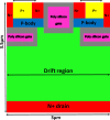
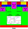
This paper analyses the various properties that governs a power MOSFET for a novel and unique vertical triple gate selective buried trench power MOSFET. Our recent work consists of a MOSFET having two lateral selective buried gates and a single vertical trench gate facing the drift region, resulting in a Triple gate power MOSFET (TGSBTPMOS). This unique combination of three gates results in significantly high device ON-state current and ultra-low ON resistance of about 0.38 mΩ.cm² in the voltage class of 78.8 V. Our proposed device has multiple inversion layers, which helps in enlarging the channel width and on-current of the device, resulting in better static state and switching performance compared to the conventional power MOSFET. 2-D Silvaco ATLAS simulation output has revealed the outperformance of the proposed device in all the areas governing power MOSFET, i.e., gate-to-drain charge (Qgd), device transfer and output (I-V) characteristic, Balliga's Figure of Merits (FOM1 and FOM2). Furthermore, the proposed device achieves 4.86 orders of magnitude improvement in FOM1, 68.85% in Ron.sp, 94.54% in Qgd, and 98.34% in FOM2. Our proposed device is an enhancement in the existing state of the art and competes with the reported power MOSFET structure in terms of performance.
© 2025. The Author(s).
Conflict of interest statement
Declarations. Competing interests: The authors declare no competing interests.
Figures





References
-
- Zhang, Y., Udrea, F. & Wang, H. Multidimensional device architectures for efficient power electronics. Nat. Electron.5, 723–734. 10.1038/s41928-022-00860-5 (2022).
-
- Vitezslav & Benda Power semiconductor devices and integrated circuits. Microelectron. J.39, 849–850 (2008).
-
- Zhu, M., Ma, J., Nela, L. & Matioli, E. High-performance normally-off tri-gate GaN power MOSFETs, Proceedings of the 31st International Symposium on Power Semiconductor Devices and ICs, May 19–23, (Shanghai, China, 2019)
-
- Cooper, J. & Islam, N. Vertical Tri-Gate power mosfets 4H-SiC. Mater. Sc Forum, ISSN:1662–9752, 924, 680–683 10.4028/www.scientific.net/MSF.924.680 (2018).
LinkOut - more resources
Full Text Sources
Miscellaneous

